This thread has been locked.

If you have a related question, please click the "Ask a related question" button in the top right corner. The newly created question will be automatically linked to this question.

AM3505: powering up sequence

Part Number: AM3505
Other Parts Discussed in Thread: AM3517

Hi team,


My customer is considering using TPS650732RSLR as PMIC for AM3505. I’ve got an inquiry on the powering up sequence, could you take a look below?


On the Application note (SLVA411), sequencing order is listed on the table 1. It has VDDSHV (3.3V) before VDDS_SRAM_CORE_BG and VDDS_SRAM_MPU.

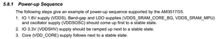
On the other hand, in section 5.8.1 on the datasheet of AM3505 has example of powering up VDDS_SRAM_CORE_BG and VDDS_SRAM_MPU before the VDDSHV (3.3V).


Which one is correct? The datasheet says “an example”, so the sequencing order of VDDSHV and VDDS_SRAM doesn’t really matter?


Best regards,

Kurumi

  • Hi Kurumi,

    Other use cases may have been demonstrated as functional, but from a AM35xx perspective the golden reference to follow for the power sequence is defined in the datasheet. Furthermore it sounds like you are setting the IO group to at least 3v3 mode (not just 1v8), so the NOTE at the bottom may not apply here.

    I would bring up the VDDSHVx, for 3v3 IO supplies after the VDDS supplies and before the VDD_CORE supply.

    " 5.8.1 Power-up Sequence The following steps give an example of power-up sequence supported by the AM3517/05.

    1. IO 1.8V supply (VDDS), Band-gap and LDO supplies (VDDS_SRAM_CORE_BG, VDDS_SRAM_MPU) and oscillator supply (VDDSOSC) should come up first to a stable state.

    2. IO 3.3V (VDDSHV) supply should be ramped up next to a stable state.

    3. Core (VDD_CORE) supply follows next to a stable state.

    4. All the PLL supplies (VDDS_DPLL_PER_CORE, VDDS_DPLL_MPU_USBHOST) and 1.8 V complex IO supplies (VDDA_DAC, VDDA1P8V_USBPHY) should be ramped up next to a stable state.

    5. Finally, 3.3 V complex IO (VDDA_3P3V_USBPHY) should be ramped up.

    6. sys_nrespwron must be held low at the time the power supplies are ramped up till the time the sys_32k and sys_xtalin clocks are stable.

    Note: In VDDSHV 1.8 V operation mode, VDDSHV can be grouped and powered up together with VDDS, VDDS_SRAM_CORE_BG, VDDS_SRAM_MPU and VDDSOSC."

    Regards,

    Colin

  • Hi Colin,


    Thank you for the reply. So, following the datasheet is the recommended method, right?

    Datasheet has “VDDS_SRAM_CORE_BG0” & “VDDS_SRAM_MPU”'s ON timing as the same with the one of VDDS. On the other hand, SLVA411 has those timing as the same with the one of VDDSHV. I believe powering up “VDDS_SRAM_CORE_BG0” & “VDDS_SRAM_MPU” at the same time with VDDS. (Please correct me if that is wrong.)

    To do so, should we connect LDO-enable with VDDS (PMIC-DCDC1 output)?


    Best regards,

    Kurumi

  • Hi Kurumi,

    Your understanding is correct.

    Regards,

    Colin