This thread has been locked.

If you have a related question, please click the "Ask a related question" button in the top right corner. The newly created question will be automatically linked to this question.

AM4372: AM4372 - VDDS3P3V_IOLDO usage

Part Number: AM4372

Hi,

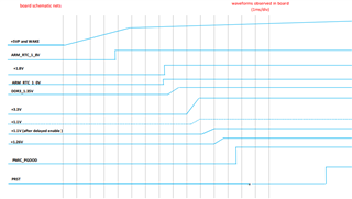
We have  AM4372 based PCB which is designed to follow normal power-up sequence as described in sec. 5.12.1.2 of datasheet.

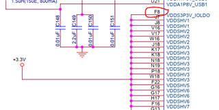
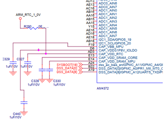
In the board, pin#F8 (VDDS3P3V_IOLDO) is connected to 3.3V supply, but pin#D6 (CAP_VDDS1P8V_IOLDO) is not connected to VDDS or VDDS_CLOCKOUT or any other load in the board.

VDDS , VDDS_CLOCKOUT are powered from a separate 1.8V supply

We are using LTC3676-1 as the PMIC.

Is it OK to connect VDDS3P3V_IOLDO to 3.3V but powering VDDS and  VDDS_CLOCKOUT from a separate source in normal power-up sequence ?

Regards,

Thomas Joseph

  • Hello Thomas Joseph

    Thank you for the query.

    Please share the PDF schematics.

    Do you have a sequence diagram.

    Our recommendation is to follow the datasheet recommended sequencing 

    Can you share the information on the EVM that you have referred.

    Regards,

    Sreenivasa

  • Dear Sir,

    Thanks for reply.

    I have sent the schematic through PM (new version of the board).

    The sequence diagram is attached for your reference.

    We started the design by referring AM4372_GP_EVM, but with some deviations.(mentioned in sequence diagram)

    Kindly review and give suggestions.

    Here is a brief history.

    We have assemble six boards in two versions. Slight change in reset mechanism across versions

    In the first version, two boards are perfectly working. In the third board, we are able to flash uboot and linux. but while booting, it halt at "booting from linux"

    In the second version of  three boards we could load Linux in one board and seems all peripherals are working.

    We could flash Linux in second board also, but after few days, the booting seems not progressing. While checking with ROM booting in UART, the "C" character is coming but it got stuck while loading u-boot spl tthrough x-modem protocol.

    The third board does not show the ROM boot character at UART terminal at all.

    Also noticed that board 2 and 3 are taking slightly more current from the input supply (5V).

    Later , we observed short in 3.3V rail and identified that the processor got damaged.(we replaced the processor)

    After isolating supplies to processor , on a detailed examination, we observed that 1.1V is rising along with 3.3V. ( Is it a problem ? )

    Hence we added delay in enable of 1.1V so that the output starts rising only after 3.3V settles to final value.(Still not tested by powering processor)

    We are waiting for your recommendations to power up the processor and continue testing

    Regards,

    Thomas Joseph

    Sequence_Diagram1.pdfSequence_Diagram1.xlsx

  • Hello Thomas Joseph

    Thank you for the inputs.

    I have reached out to the device expert for his comments. 

    FYI, TI recommends following the power sequence and also choosing the power sequence based on the system requirements from the below section.

    5.12.1.2 Power-Up Sequencing

    It is important for follow the power supply ramp and slew recommendations. In the PDF ramp diagram that you shared, i see some of the supplies ramping fast and may not be recommended. 

    Figure 5-3. Power Supply Slew and Slew Rate

    Pls refer below data sheet for more details.

    https://www.ti.com/lit/ds/symlink/am4372.pdf

    Regards,

    Sreenivasa

  • Dear Sir,

    Thanks for the details.

    Here is the screenshot of 1.8V to VDDS. Datasheet recommendation is >18usec. We observe around 200usec.

    Also, the screenshot corresponding to RTC supplies (1.8V and 1.0V)

    Other supplies (1.1V, 1.26V, 3.3V, 1.35V) ramp not faster than 1ms

    Are these ramp time sufficient ?

    Kindly give suggestions.

    Regards,

    Thomas Joseph

  • Hello Thomas, 

    Thank you for the inputs.

    Can you help me understand the timing diagram that you are looking to follow with reference to the datasheet.

    Examples 

    Figure 5-6. Power Sequencing With RTC Feature Enabled, Dual-Voltage IOs Configured as 1.8 V, 3.3 V

    Can you also map the supply rails you mentioned in the timing diagram to the names in the datasheet sequencing diagram.

    Following the supply ramp recommendations in the data sheet and ensuring the next supply ramps after the ramp time should be fine.

    Are these ramp time sufficient ?

    .  I can see a 1.1V power rail named ARM_RTC_1_0V that is ramping early.

    Please review and make sure you follow the datasheet recommendations.

    Regards,

    Sreenivasa

  • Dear Sir,

    Thanks for the reply.

    Kindly find the timing diagram attached. In the diagram, the schematic nets, voltage ramp observed in the board, mapping to AM4372 supply rails are detailed.

    The design is based on the timing diagram in the datasheet " Figure 5-4 Power Sequencing with RTC Feature Enabled, Dual IOs configured as 3.3V"

    There are few deviations, which are mentioned under Notes in the attached timing diagram

    Kindly note that ARM_RTC_1_0V is a 1.0V supply and is connected to CAP_VDD_RTC of AM4372(RTC core supply)

    Kindly let me know if the sequencing observed in the board has any violations.

    Regards,

    Thomas Joseph

    1121.Sequence_Diagram1.pdf

  • Hello Thomas Joseph

    Thank you.

    Please verify the note below for the CAP_VDD_RTC supply voltage and configuration. Where did the 1V come from?

    A. The CAP_VDD_RTC terminal operates as an input to the RTC core voltage domain when the internal RTC LDO is disabled by connecting the RTC_KALDO_ENn terminal to VDDS_RTC. If the internal RTC LDO is disabled, CAP_VDD_RTC should be sourced from an external 1.1-V power supply. If CAP_VDD_RTC is ramped after VDD_CORE, there might be a small amount of additional leakage current on VDD_CORE. VDDS_RTC can be ramped independent of other supplies if RTC_PMIC_EN functionality is not required. If VDDS_RTC is ramped after VDD_CORE when internal RTC LDO is enabled, there might be a small amount of leakage current on VDD_CORE.

    Regards,

    Sreenivasa

  • Dear Sir,

    Here are the answers related to RTC power rails.

    RTC_KALDO_ENn terminal is connected to to VDDS_RTC ( ARM_RTC_1_8V ), hence internal regulator is disabled.

    CAP_VDD_RTC is from a separate LDO of PMIC which is supplying 1.0V. From datasheet, the range of  CAP_VDD_RTC supply range is 0.9V - 1.25V. Hence we understand that a supply of 1.0V is safe.

    In the design, CAP_VDD_RTC is ramped before VDD_CORE.

    RTC_PMIC_EN is floating in the design

    Kindly give suggestions .

    Regards,

    Thomas Joseph

  • Hello Thomas Joseph

    Thank you. 

    Please note that have not defined a time between ramps.  We are only concerned with potential differences during supply ramp. 

    Do ensure you are following the data sheet power supply ramp requirements and also have the recommended supply caps as per section 5.11 External Capacitors

    Regards,

    Sreenivasa

  • Dear Sir,

    I will check any assembly issues with decoupling capacitors.

    Will you please explain the statement   "Please note that have not defined a time between ramps.  We are only concerned with potential differences during supply ramp."

    Regards,

    Thomas Joseph

  • Hello Thomas Joseph

    Thank you.

    You provided the previous information as below

    Here is the screenshot of 1.8V to VDDS. Datasheet recommendation is >18usec. We observe around 200usec.

    Other supplies (1.1V, 1.26V, 3.3V, 1.35V) ramp not faster than 1ms.

    If you look at the sequence diagram, you may have a question on the time required for the next supply to ramp after the previous supply has ramped.

    Refer below. answer:

    Please note that have not defined a time between ramps.  We are only concerned with potential differences during supply ramp.

    Regards,

    Sreenivasa

  • Hello Thomas Joseph,

    Checking if you were able to make progress.

    Regards,

    Sreenivasa