This thread has been locked.

If you have a related question, please click the "Ask a related question" button in the top right corner. The newly created question will be automatically linked to this question.

AM62X-PET-CALC: CSI waveform review

Part Number: AM62X-PET-CALC

Hi TI 

As you know , we can't test the SOC die side wavefrom but can only test the CSI nearest test point nearby SOC.

We found the waveform of CSI has non-monotonicity rising edge at nearby SOC side test point, whether this is ok from TI view?

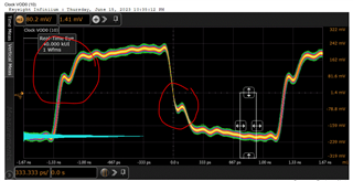
What's more CSI lane compliance test is pass, report also attached.

L0.pdf

BR Jingcheng

  • Hi TI

    Any  update from TI ?

    BR Jingcheng

  • BR Jingcheng,

    Quick question. Are you using TI SK board or custom board.

    Thanks

    Yogesh

  • Hi Yogesh

    Test under Customer board.

    BR Jingcheng

  • Hello Jingcheng,

    Please refer below inputs i received from the device expert.

    An LVCMOS signal will have a step function on the voltage transition at the source end of a signal trace based on its AC characteristic impedance (transmission line) and the drivers output impedance.  The step occurs because the output buffer’s source impedance is driving a transmission line with a specific AC characteristic impedance and the resulting voltage at the source end of the signal trace will be the voltage divider of the two impedances.  For example, the voltage step would occur at VDD/2 if the output buffer impedance is equal to the signal trace impedance.  The step voltage will remain at the source end of the signal trace until the signal propagates to the far end, which is high impedance.  The far end of the signal trace is connected to a high impedance load and the impedance change creates an in-phase reflection the returns to the source.  Once the reflection returns to the source, its voltage will continue to rise.  The time the step function is present at the source represents the time it takes for the signal to propagate to the far end of the signal trace and the reflect to return to the source.  The far end does not see the voltage step since the in-phase reflection instantly sums with the incident signal.

     I suspect most of the non-monotonic behavior observed by the scope is not real and is being caused by too much inductance in the scope probe ground.

    Regards,

    Sreenivasa