Because of the holidays, TI E2E™ design support forum responses will be delayed from Dec. 25 through Jan. 2. Thank you for your patience.

This thread has been locked.

If you have a related question, please click the "Ask a related question" button in the top right corner. The newly created question will be automatically linked to this question.

TMDSICE3359: How user control GPMC address via GPIO

Part Number: TMDSICE3359

Hello,

Let me confirm meaning of GPIO2_12 and 2_13 of ICE board version 2.1.
According to following user's guide, it seems that above two are for GPMC_A18 and A19 of NOR flash.
https://www.ti.com/jp/lit/ug/spruip3/spruip3.pdf

However, it seems that these are set as GPIO not GPMC.
Then I have following questions ?

Q1. Is my above understanding that signal "gpio2_12" and "gpio2_13" are set as GPIO correct ?
Q2. If so, is there any information how you control these gpios as address function of GPMC ?

BR,

  • Hi Machida-san,

    I am routing your query to our hardware expert for comments.

  • Hi Machida-san,

    I am assigning to the GPMC expert.

    Regards,

    Sreenivasa

  • Hi Machida-san,

    I'm not 100% certain what the board designer intended here. Probably that these GPIO2_12 and 2_13  pins would be configured as GPIOs in the pinmux and set manually before trying to write/read from the upper address ranges of the NOR flash. For example, 1) check address to be accessed with software before writing or reading from it, 2) Set GPIOs with software to match the values of A18/A19, 3) Write or read from NOR flash.

    Alternately, these gpios can carry GPMC address bits A21 and A22 in address/data mux mode (which is being used with this NOR flash), so you could configure the pins as GPMC in pinmux and access the address range that drives A21/A22 as 1's. there will be a hole in the memory range since A18 - A20 are not connected to the NOR flash, but it should work. GPMC has a 512MB memory map in the system which is large enough to get upto these A21/A22 bits...

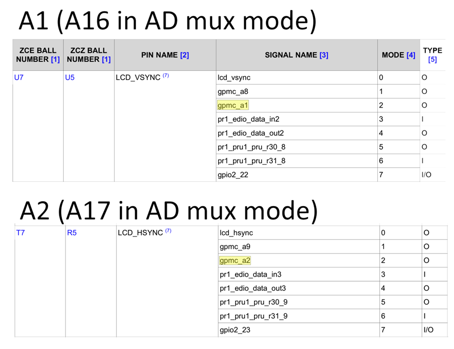
    See below screenshots of TRM and datasheet. You can see how A1 and A2 pins are carrying A16 and A17 addresses to the NOR in this AD mux mode.
    It would have been ideal if the board designer could have used pins A3 and A4 to carry A18 and A19 to the NOR flash for a continuous address space, but I supposed those pins were consumed already in the board design. So they gave you GPIO2_12 and 2_13 instead and left it up to the software to make it work. Pin mux tradeoffs must be considered with any board design.

    Hope this helps,
    Mark

  • Hello Mark-san,

    Thank you for your opinion.
    Umm, I understand that it is difficult to understand why designer configure like this..

    I also have same question for "GPMC_NOR_A1" and "GPMC_NOR_A2".
    It also seems that these two are controled by GPIO.
    However, there is no description about this in user's guide of ICE board.

    Do you know which function is assigned to these two on AM335X ?
    (I checked "am335x-icev2.dts" from github to check configuration of above pins, but there is no description. So I assume these are going to be used as GPIO.)
    https://github.com/ARM-software/u-boot/blob/master/arch/arm/dts/am335x-icev2.dts

    BR,

  • Hi Machida-san,

    I also have same question for "GPMC_NOR_A1" and "GPMC_NOR_A2".

    these A1 and A2 pins can be driven from GPMC. They don't need to be configured as GPIOs.

    See previous post where the pinmux shows that LCD_VSYNC can select GPMC_A1, which in AD-mux mode will output A16 address. Similarly, LCD_HSYNC can select GPMC_A2, which in AD-mux mode will output A17. I added this part of the pinmux table below.

    Do you know which function is assigned to these two on AM335X ?

    I don't see this pinmux selection in the .dts file (https://github.com/ARM-software/u-boot/blob/master/arch/arm/dts/am335x-icev2.dts).

    But I also do not see any NOR-related pinmux either... Maybe this .dts does not support the NOR? Lets loop in SW expert to see how the NOR is configured by .dts.

    Regards,
    Makr

  • am335x-icev2.dts doesn't enable GPMC interface. So all these pins are in the default pinmux mode if they are not specifically changed in am335x-icev2.dtsi.

  • Hello Bin-san and Mark-san,

    Thank you for your reply.
    Understood.
    Finally, I would like you to ask whether you have experience such as following usecase support.

    * Customer need to change larger NOR flash product due to EOL of smaller NOR flash product on their custom board.

    1. Have you ever heard above usecase ?
    2. If yes, have you ever supported something ?
    3. If yes, could you please share support contents as you can disclose as possible ?

    BR,

  • Hi Machida-san,

    I will defer to Mark to comment on your questions.

  • Hi Machida-san,

    I've heard of customers needing to change to larger NOR flash due to EOL of smaller one.

    If they don't need to utilize the additional capacity, they could terminate the upper address bits to GND.

    We've supported this request but I could not find any E2E about it. The idea of configuring GPIOs for upper address pins is feasible, but I cannot find an example.

    I did however find this E2E that shows some DTS configuration for NOR flash on ICE board (without configuring any pins):

    https://e2e.ti.com/support/processors-group/processors/f/processors-forum/521445/am3359-icev2-nor-flash-gpmc-settings

    How much capacity of the NOR flash does the customer need to utilize?

    EDIT- adding 2 more links

    https://e2e.ti.com/support/processors-group/processors/f/processors-forum/354942/am335x-nor-flash---256mb-issue

    https://e2e.ti.com/support/processors-group/processors/f/processors-forum/834921/am3352-nor-boot-support-in-u-boot

    Regards,
    Mark

  • Hello,

    Thank you for your reply.
    >We've supported this request but I could not find any E2E about it. 
    It's OK to send me later, but if you find something thread related to this, please let me know.

    >If they don't need to utilize the additional capacity, they could terminate the upper >address bits to GND.
    >How much capacity of the NOR flash does the customer need to utilize?
    Currently, it may be enough to use small size capacity. so do not need to expand capacity.
    Is my understanding that description for upper address termination is for AM335X side correct ?

    BR,

  • Currently, it may be enough to use small size capacity. so do not need to expand capacity.
    Is my understanding that description for upper address termination is for AM335X side correct ?

    I meant that they could terminate the upper address bits on the NOR side, if they do not want to connect them to GPIOs on the AM335x side. this would prevent addressing the full capacity of the memory.