This thread has been locked.

If you have a related question, please click the "Ask a related question" button in the top right corner. The newly created question will be automatically linked to this question.

OMAPL138B-EP: How to configure DTS for multiple NAND Flash

Part Number: OMAPL138B-EP
Other Parts Discussed in Thread: OMAPL138, OMAP-L132, DP83640

Hello, I have modified the DTS for OMAPL138 LCDK board as out custom board has 2 nand flash chip at cs 2 and cs 3. 

I have done the following but cs2 is never discovered at booting. Thanks

&aemif {
pinctrl-names = "default";
pinctrl-0 = <&nand_pins>;
status = "okay";
cs2 {
#address-cells = <2>;
#size-cells = <1>;
clock-ranges;
ranges;

ti,cs-chipselect = <2>;

nand@0,0 {
compatible = "ti,davinci-nand";
#address-cells = <1>;
#size-cells = <1>;
reg = <0 0x00000000 0x02000000
1 0x00000000 0x00008000>;

ti,davinci-chipselect = <1>;
ti,davinci-mask-ale = <0>;
ti,davinci-mask-cle = <0>;
ti,davinci-mask-chipsel = <0>;

ti,davinci-nand-buswidth = <16>;
ti,davinci-ecc-mode = "hw";
ti,davinci-ecc-bits = <4>;
ti,davinci-nand-use-bbt;

/*
* Board has 2 NAND Flash. The CS2 NAND FLash
*/
partitions {
compatible = "fixed-partitions";
#address-cells = <1>;
#size-cells = <1>;

partition@0 {
label = "FPGA FW";
reg = <0 0x200000>;
};
partition@200000 {
/* Extra partition */
label = "Spare";
reg = <0x0200000 0>;
};
};
};
};

cs3 {
#address-cells = <2>;
#size-cells = <1>;
clock-ranges;
ranges;

ti,cs-chipselect = <3>;

nand@2000000,0 {
compatible = "ti,davinci-nand";
#address-cells = <1>;
#size-cells = <1>;
reg = <0 0x02000000 0x02000000
1 0x00000000 0x00008000>;

ti,davinci-chipselect = <1>;
ti,davinci-mask-ale = <0>;
ti,davinci-mask-cle = <0>;
ti,davinci-mask-chipsel = <0>;

ti,davinci-nand-buswidth = <16>;
ti,davinci-ecc-mode = "hw";
ti,davinci-ecc-bits = <4>;
ti,davinci-nand-use-bbt;

/*
* The OMAP-L132/L138 Bootloader doc SPRAB41E reads:
* "To boot from NAND Flash, the AIS should be written
* to NAND block 1 (NAND block 0 is not used by default)".
* The same doc mentions that for ROM "Silicon Revision 2.1",
* "Updated NAND boot mode to offer boot from block 0 or block 1".
* However the limitation is left here by default for compatibility
* with older silicon and because it needs new boot pin settings
* not possible in stock LCDK.
*/
partitions {
compatible = "fixed-partitions";
#address-cells = <1>;
#size-cells = <1>;

partition@0 {
label = "u-boot env";
reg = <0 0x020000>;
};
partition@20000 {
/* The LCDK defaults to booting from this partition */
label = "u-boot";
reg = <0x020000 0x080000>;
};
partition@100000 {
/* FPGA FW Settings */
label = "FPGA FW Settings";
reg = <0x100000 0x020000>;
};
partition@120000 {
/* FPGA FW */
label = "FPGA FW";
reg = <0x120000 0x200000>;
};
partition@320000 {
label = "free space";
reg = <0x320000 0>;
};
};
};
};
};

  • Boot log:

    root@F280Series-10-8-254-254:~# dmesg
    [ 1.364803] gpio gpiochip0: (davinci_gpio.0): created GPIO range 95->95 ==> 1c14120.pinmux PIN 88->88
    [ 1.364952] gpio gpiochip0: (davinci_gpio.0): created GPIO range 96->96 ==> 1c14120.pinmux PIN 158->158
    [ 1.365101] gpio gpiochip0: (davinci_gpio.0): created GPIO range 97->97 ==> 1c14120.pinmux PIN 157->157
    [ 1.365250] gpio gpiochip0: (davinci_gpio.0): created GPIO range 98->98 ==> 1c14120.pinmux PIN 156->156
    [ 1.365397] gpio gpiochip0: (davinci_gpio.0): created GPIO range 99->99 ==> 1c14120.pinmux PIN 155->155
    [ 1.365549] gpio gpiochip0: (davinci_gpio.0): created GPIO range 100->100 ==> 1c14120.pinmux PIN 154->154
    [ 1.365705] gpio gpiochip0: (davinci_gpio.0): created GPIO range 101->101 ==> 1c14120.pinmux PIN 129->129
    [ 1.365857] gpio gpiochip0: (davinci_gpio.0): created GPIO range 102->102 ==> 1c14120.pinmux PIN 113->113
    [ 1.366015] gpio gpiochip0: (davinci_gpio.0): created GPIO range 103->103 ==> 1c14120.pinmux PIN 112->112
    [ 1.366172] gpio gpiochip0: (davinci_gpio.0): created GPIO range 104->104 ==> 1c14120.pinmux PIN 111->111
    [ 1.366330] gpio gpiochip0: (davinci_gpio.0): created GPIO range 105->105 ==> 1c14120.pinmux PIN 110->110
    [ 1.366490] gpio gpiochip0: (davinci_gpio.0): created GPIO range 106->106 ==> 1c14120.pinmux PIN 109->109
    [ 1.366652] gpio gpiochip0: (davinci_gpio.0): created GPIO range 107->107 ==> 1c14120.pinmux PIN 108->108
    [ 1.366815] gpio gpiochip0: (davinci_gpio.0): created GPIO range 108->108 ==> 1c14120.pinmux PIN 107->107
    [ 1.367317] gpio gpiochip0: (davinci_gpio.0): created GPIO range 109->109 ==> 1c14120.pinmux PIN 106->106
    [ 1.367536] gpio gpiochip0: (davinci_gpio.0): created GPIO range 110->110 ==> 1c14120.pinmux PIN 105->105
    [ 1.367718] gpio gpiochip0: (davinci_gpio.0): created GPIO range 111->111 ==> 1c14120.pinmux PIN 104->104
    [ 1.367917] gpio gpiochip0: (davinci_gpio.0): created GPIO range 112->112 ==> 1c14120.pinmux PIN 145->145
    [ 1.368095] gpio gpiochip0: (davinci_gpio.0): created GPIO range 113->113 ==> 1c14120.pinmux PIN 144->144
    [ 1.368267] gpio gpiochip0: (davinci_gpio.0): created GPIO range 114->114 ==> 1c14120.pinmux PIN 143->143
    [ 1.368440] gpio gpiochip0: (davinci_gpio.0): created GPIO range 115->115 ==> 1c14120.pinmux PIN 142->142
    [ 1.368609] gpio gpiochip0: (davinci_gpio.0): created GPIO range 116->116 ==> 1c14120.pinmux PIN 141->141
    [ 1.368780] gpio gpiochip0: (davinci_gpio.0): created GPIO range 117->117 ==> 1c14120.pinmux PIN 140->140
    [ 1.368951] gpio gpiochip0: (davinci_gpio.0): created GPIO range 118->118 ==> 1c14120.pinmux PIN 139->139
    [ 1.369126] gpio gpiochip0: (davinci_gpio.0): created GPIO range 119->119 ==> 1c14120.pinmux PIN 138->138
    [ 1.369300] gpio gpiochip0: (davinci_gpio.0): created GPIO range 120->120 ==> 1c14120.pinmux PIN 137->137
    [ 1.369479] gpio gpiochip0: (davinci_gpio.0): created GPIO range 121->121 ==> 1c14120.pinmux PIN 136->136
    [ 1.369654] gpio gpiochip0: (davinci_gpio.0): created GPIO range 122->122 ==> 1c14120.pinmux PIN 135->135
    [ 1.369830] gpio gpiochip0: (davinci_gpio.0): created GPIO range 123->123 ==> 1c14120.pinmux PIN 134->134
    [ 1.370007] gpio gpiochip0: (davinci_gpio.0): created GPIO range 124->124 ==> 1c14120.pinmux PIN 133->133
    [ 1.370188] gpio gpiochip0: (davinci_gpio.0): created GPIO range 125->125 ==> 1c14120.pinmux PIN 132->132
    [ 1.370367] gpio gpiochip0: (davinci_gpio.0): created GPIO range 126->126 ==> 1c14120.pinmux PIN 131->131
    [ 1.370547] gpio gpiochip0: (davinci_gpio.0): created GPIO range 127->127 ==> 1c14120.pinmux PIN 130->130
    [ 1.370730] gpio gpiochip0: (davinci_gpio.0): created GPIO range 128->128 ==> 1c14120.pinmux PIN 159->159
    [ 1.370915] gpio gpiochip0: (davinci_gpio.0): created GPIO range 129->129 ==> 1c14120.pinmux PIN 31->31
    [ 1.371099] gpio gpiochip0: (davinci_gpio.0): created GPIO range 130->130 ==> 1c14120.pinmux PIN 30->30
    [ 1.371283] gpio gpiochip0: (davinci_gpio.0): created GPIO range 131->131 ==> 1c14120.pinmux PIN 20->20
    [ 1.371468] gpio gpiochip0: (davinci_gpio.0): created GPIO range 132->132 ==> 1c14120.pinmux PIN 28->28
    [ 1.371653] gpio gpiochip0: (davinci_gpio.0): created GPIO range 133->133 ==> 1c14120.pinmux PIN 27->27
    [ 1.371842] gpio gpiochip0: (davinci_gpio.0): created GPIO range 134->134 ==> 1c14120.pinmux PIN 26->26
    [ 1.372030] gpio gpiochip0: (davinci_gpio.0): created GPIO range 135->135 ==> 1c14120.pinmux PIN 23->23
    [ 1.372217] gpio gpiochip0: (davinci_gpio.0): created GPIO range 136->136 ==> 1c14120.pinmux PIN 153->153
    [ 1.372409] gpio gpiochip0: (davinci_gpio.0): created GPIO range 137->137 ==> 1c14120.pinmux PIN 152->152
    [ 1.372600] gpio gpiochip0: (davinci_gpio.0): created GPIO range 138->138 ==> 1c14120.pinmux PIN 151->151
    [ 1.372792] gpio gpiochip0: (davinci_gpio.0): created GPIO range 139->139 ==> 1c14120.pinmux PIN 150->150
    [ 1.372987] gpio gpiochip0: (davinci_gpio.0): created GPIO range 140->140 ==> 1c14120.pinmux PIN 149->149
    [ 1.373182] gpio gpiochip0: (davinci_gpio.0): created GPIO range 141->141 ==> 1c14120.pinmux PIN 148->148
    [ 1.373376] gpio gpiochip0: (davinci_gpio.0): created GPIO range 142->142 ==> 1c14120.pinmux PIN 147->147
    [ 1.373574] gpio gpiochip0: (davinci_gpio.0): created GPIO range 143->143 ==> 1c14120.pinmux PIN 146->146
    [ 1.374580] gpio gpiochip0: (davinci_gpio.0): added GPIO chardev (254:0)
    [ 1.375064] gpiochip_setup_dev: registered GPIOs 0 to 143 on device: gpiochip0 (davinci_gpio.0)
    [ 1.378495] edma 1c00000.edma: memcpy is disabled
    [ 1.394092] edma 1c00000.edma: TI EDMA DMA engine driver
    [ 1.399934] davinci_mmc 1c40000.mmc: GPIO lookup for consumer cd
    [ 1.399976] davinci_mmc 1c40000.mmc: using device tree for GPIO lookup
    [ 1.400115] of_get_named_gpiod_flags: parsed 'cd-gpios' property of node '/soc@1c00000/mmc@40000[0]' - status (0)
    [ 1.400244] gpio-65 (cd): gpiod_set_debounce: missing set() or set_config() operations
    [ 1.400284] davinci_mmc 1c40000.mmc: Got CD GPIO
    [ 1.403680] davinci_mmc 1c40000.mmc: GPIO lookup for consumer wp
    [ 1.403703] davinci_mmc 1c40000.mmc: using device tree for GPIO lookup
    [ 1.403779] of_get_named_gpiod_flags: can't parse 'wp-gpios' property of node '/soc@1c00000/mmc@40000[0]'
    [ 1.403847] of_get_named_gpiod_flags: can't parse 'wp-gpio' property of node '/soc@1c00000/mmc@40000[0]'
    [ 1.403885] davinci_mmc 1c40000.mmc: using lookup tables for GPIO lookup
    [ 1.403915] davinci_mmc 1c40000.mmc: No GPIO consumer wp found
    [ 1.431185] davinci_mmc 1c40000.mmc: Using DMA, 4-bit mode
    [ 1.447624] console [netcon0] enabled
    [ 1.450243] netconsole: network logging started
    [ 1.455386] davinci_emac 1e20000.ethernet: incompatible machine/device type for reading mac address
    [ 1.469094] hctosys: unable to open rtc device (rtc0)
    [ 1.474479] ALSA device list:
    [ 1.476187] No soundcards found.
    [ 1.492395] Waiting for root device PARTUUID=17b37261-02...
    [ 1.496910] mmc0: host does not support reading read-only switch, assuming write-enable
    [ 1.505923] mmc0: new high speed SDHC card at address 59b4
    [ 1.513521] mmcblk0: mmc0:59b4 USD00 29.5 GiB
    [ 1.521158] mmcblk0: p1 p2 p3
    [ 1.572686] random: fast init done
    [ 1.621859] EXT4-fs (mmcblk0p2): mounted filesystem with ordered data mode. Opts: (null)
    [ 1.629066] VFS: Mounted root (ext4 filesystem) on device 179:2.
    [ 1.662917] devtmpfs: mounted
    [ 1.666030] Freeing unused kernel memory: 260K
    [ 1.669397] This architecture does not have kernel memory protection.
    [ 1.674591] Run /sbin/init as init process
    [ 2.422024] systemd[1]: System time before build time, advancing clock.
    [ 2.620025] systemd[1]: systemd 239 running in system mode. (+PAM -AUDIT -SELINUX +IMA -APPARMOR +SMACK +SYSVINIT +UTMP -LIBCRYPTSETUP -GCRYPT -GNUTLS +ACL +XZ -LZ4 -SECCOMP +BLKID -ELFUTILS +KMOD -IDN2 -IDN -PCRE2 default-hierarchy=hybrid)
    [ 2.643266] systemd[1]: Detected architecture arm.
    [ 2.730171] systemd[1]: Set hostname to <F280Series-10-8-254-254>.
    [ 3.893768] systemd[1]: File /lib/systemd/system/systemd-journald.service:36 configures an IP firewall (IPAddressDeny=any), but the local system does not support BPF/cgroup based firewalling.
    [ 3.910182] systemd[1]: Proceeding WITHOUT firewalling in effect! (This warning is only shown for the first loaded unit using IP firewalling.)
    [ 4.646275] systemd[1]: Configuration file /etc/systemd/system/www-coda-init.service is marked executable. Please remove executable permission bits. Proceeding anyway.
    [ 4.865550] systemd[1]: serial-getty@ttyS2.service: Service lacks both ExecStart= and ExecStop= setting. Refusing.
    [ 5.472577] systemd[1]: serial-getty@ttyS2.service: Cannot add dependency job, ignoring: Unit serial-getty@ttyS2.service has a bad unit file setting.
    [ 5.510987] random: systemd: uninitialized urandom read (16 bytes read)
    [ 5.518723] systemd[1]: Listening on initctl Compatibility Named Pipe.
    [ 5.558023] random: systemd: uninitialized urandom read (16 bytes read)
    [ 5.576488] systemd[1]: Created slice User and Session Slice.
    [ 5.618073] random: systemd: uninitialized urandom read (16 bytes read)
    [ 6.553125] cryptodev: loading out-of-tree module taints kernel.
    [ 6.598909] cryptodev: driver 1.9 loaded.
    [ 6.941474] EXT4-fs (mmcblk0p2): re-mounted. Opts: (null)
    [ 7.667731] systemd[1]: Started Load Kernel Modules.
    [ 7.682049] systemd[1]: Mounted Kernel Debug File System.
    [ 7.798615] systemd[1]: Started Create list of required static device nodes for the current kernel.
    [ 7.907840] systemd[1]: Started Remount Root and Kernel File Systems.
    [ 7.940867] systemd[1]: rngd.service: Main process exited, code=exited, status=1/FAILURE
    [ 7.972427] systemd[1]: rngd.service: Failed with result 'exit-code'.
    [ 8.040477] systemd[1]: Mounted Temporary Directory (/tmp).
    [ 8.213943] systemd[1]: Starting Create Static Device Nodes in /dev...
    [ 8.401912] systemd[1]: Mounting Kernel Configuration File System...
    [ 8.602462] systemd[1]: Starting Apply Kernel Variables...
    [ 11.599205] systemd-journald[76]: Received request to flush runtime journal from PID 1
    [ 20.184340] davinci-rproc 11800000.dsp: assigned reserved memory node dsp-memory@c3000000
    [ 20.319148] remoteproc remoteproc0: dsp is available
    [ 20.325766] remoteproc remoteproc0: Direct firmware load for rproc-dsp-fw failed with error -2
    [ 20.443005] remoteproc remoteproc0: powering up dsp
    [ 20.446852] remoteproc remoteproc0: Direct firmware load for rproc-dsp-fw failed with error -2
    [ 20.575668] remoteproc remoteproc0: request_firmware failed: -2
    [ 20.652001] nand: No NAND device found
    [ 20.783558] nand: device found, Manufacturer ID: 0x2c, Chip ID: 0xcc
    [ 20.868490] nand: Micron MT29F4G16ABADAH4
    [ 20.871276] nand: 512 MiB, SLC, erase size: 128 KiB, page size: 2048, OOB size: 64
    [ 21.010590] Bad block table not found for chip 0
    [ 21.157328] Bad block table not found for chip 0
    [ 21.160706] Scanning device for bad blocks
    [ 22.870642] omap_rtc 1c23000.rtc: already running
    [ 22.968381] omap_rtc 1c23000.rtc: char device (253:0)
    [ 22.968475] omap_rtc 1c23000.rtc: registered as rtc0
    [ 25.882663] Bad block table written to 0x00001ffe0000, version 0x01
    [ 25.979021] Bad block table written to 0x00001ffc0000, version 0x01
    [ 25.984332] 5 fixed-partitions partitions found on MTD device 62000000.nand
    [ 26.159351] Creating 5 MTD partitions on "62000000.nand":
    [ 26.163551] 0x000000000000-0x000000020000 : "u-boot env"
    [ 26.289726] 0x000000020000-0x0000000a0000 : "u-boot"
    [ 26.331805] 0x000000100000-0x000000120000 : "FPGA FW Settings"
    [ 26.398563] 0x000000120000-0x000000320000 : "FPGA FW"
    [ 26.498497] 0x000000320000-0x000020000000 : "free space"
    [ 26.657644] davinci_nand 62000000.nand: controller rev. 2.5
    [ 27.001358] davinci_mdio 1e24000.mdio: resetting idled controller
    [ 27.192717] NatSemi DP83640 1e24000.mdio:01: attached PHY driver [NatSemi DP83640] (mii_bus:phy_addr=1e24000.mdio:01, irq=POLL)
    [ 27.355185] IPv6: ADDRCONF(NETDEV_UP): eth0: link is not ready
    [ 29.368818] davinci_emac 1e20000.ethernet eth0: Link is Up - 100Mbps/Full - flow control off
    [ 29.376103] IPv6: ADDRCONF(NETDEV_CHANGE): eth0: link becomes ready
    [ 46.937344] random: crng init done
    [ 46.939507] random: 7 urandom warning(s) missed due to ratelimiting
    [ 91.899569] NET: Registered protocol family 15
    [ 95.102170] Initializing XFRM netlink socket
    [ 100.742052] EXT4-fs (mmcblk0p3): mounting ext3 file system using the ext4 subsystem
    [ 101.133774] EXT4-fs (mmcblk0p3): mounted filesystem with ordered data mode. Opts: (null)
    [ 109.696346] NET: Registered protocol family 45

  • Hi Mitesh,

    I have done the following but cs2 is never discovered at booting. Thanks

    If you only define one CS in DTS, does its NAND flash get descovered at booting?

  • HI Bin, CS3 always work but CS2 haven't manged to get it working. I am not sure about the chip select and chip select mask to be. 

  • Hi Mitesh,

    First please remove all CS3 related from DTS and get CS2 alone to work, then we will add back CS3 configs.

  • Okay, I will try this. Thanks 

  • Hi Bin, I tried removed CS3 and added in just the CS2 logic and the NAND flash was not detected on boot up. 

    Thanks 

  • In terms of hardware the both Nand flash are connected same as the omapl138-lcdk board but only difference for CS2 are

    1. Chip select is connected to CS2

    2. Wait signal (R/~B) is connected to EMA_WAIT 1 instead of EMA_WAIT 0 as for CS3. 

    Thanks 

  • Hi Mitesh,

    Please attach the device tree for the NAND devices.

    Please attach it as a file, not copy&paste which losses the indentation and makes it difficult to read.

  • Hi Bin,

    Attached. Thanks


    2311.da850.txt
    /*
     * Copyright 2012 DENX Software Engineering GmbH
     * Heiko Schocher <hs@denx.de>
     *
     * This program is free software; you can redistribute  it and/or modify it
     * under  the terms of  the GNU General  Public License as published by the
     * Free Software Foundation;  either version 2 of the  License, or (at your
     * option) any later version.
     */
    #include <dt-bindings/interrupt-controller/irq.h>
    
    / {
    	#address-cells = <1>;
    	#size-cells = <1>;
    	chosen { };
    	aliases {
    		rproc0 = &dsp;
    	};
    
    	memory@c0000000 {
    		device_type = "memory";
    		reg = <0xc0000000 0x0>;
    	};
    
    	arm {
    		#address-cells = <1>;
    		#size-cells = <1>;
    		ranges;
    		intc: interrupt-controller@fffee000 {
    			compatible = "ti,cp-intc";
    			interrupt-controller;
    			#interrupt-cells = <1>;
    			ti,intc-size = <101>;
    			reg = <0xfffee000 0x2000>;
    		};
    	};
    	clocks: clocks {
    		ref_clk: ref_clk {
    			compatible = "fixed-clock";
    			#clock-cells = <0>;
    			clock-output-names = "ref_clk";
    		};
    		sata_refclk: sata_refclk {
    			compatible = "fixed-clock";
    			#clock-cells = <0>;
    			clock-output-names = "sata_refclk";
    			status = "disabled";
    		};
    		/*usb_refclkin: usb_refclkin {
    			compatible = "fixed-clock";
    			#clock-cells = <0>;
    			clock-output-names = "usb_refclkin";
    			status = "disabled";
    		};*/
    	};
    	dsp: dsp@11800000 {
    		compatible = "ti,da850-dsp";
    		reg = <0x11800000 0x40000>,
    		      <0x11e00000 0x8000>,
    		      <0x11f00000 0x8000>,
    		      <0x01c14044 0x4>,
    		      <0x01c14174 0x8>;
    		reg-names = "l2sram", "l1pram", "l1dram", "host1cfg", "chipsig";
    		interrupt-parent = <&intc>;
    		interrupts = <28>;
    		clocks = <&psc0 15>;
    		resets = <&psc0 15>;
    		status = "disabled";
    	};
    	soc@1c00000 {
    		compatible = "simple-bus";
    		model = "da850";
    		#address-cells = <1>;
    		#size-cells = <1>;
    		ranges = <0x0 0x01c00000 0x400000>;
    		interrupt-parent = <&intc>;
    
    		psc0: clock-controller@10000 {
    			compatible = "ti,da850-psc0";
    			reg = <0x10000 0x1000>;
    			#clock-cells = <1>;
    			#reset-cells = <1>;
    			#power-domain-cells = <1>;
    			clocks = <&pll0_sysclk 1>, <&pll0_sysclk 2>,
    				 <&pll0_sysclk 4>, <&pll0_sysclk 6>,
    				 <&async1_clk>;
    			clock-names = "pll0_sysclk1", "pll0_sysclk2",
    				      "pll0_sysclk4", "pll0_sysclk6",
    				      "async1";
    		};
    		pll0: clock-controller@11000 {
    			compatible = "ti,da850-pll0";
    			reg = <0x11000 0x1000>;
    			clocks = <&ref_clk>, <&pll1_sysclk 3>;
    			clock-names = "clksrc", "extclksrc";
    
    			pll0_pllout: pllout {
    				#clock-cells = <0>;
    			};
    			pll0_sysclk: sysclk {
    				#clock-cells = <1>;
    			};
    			pll0_auxclk: auxclk {
    				#clock-cells = <0>;
    			};
    			pll0_obsclk: obsclk {
    				#clock-cells = <0>;
    			};
    		};
    		pmx_core: pinmux@14120 {
    			compatible = "pinctrl-single";
    			reg = <0x14120 0x50>;
    			#pinctrl-cells = <2>;
    			pinctrl-single,bit-per-mux;
    			pinctrl-single,register-width = <32>;
    			pinctrl-single,function-mask = <0xf>;
    			/* pin base, nr pins & gpio function */
    			pinctrl-single,gpio-range = <&range   0 17 0x8>,
    						    <&range  17  8 0x4>,
    						    <&range  26  8 0x4>,
    						    <&range  34 80 0x8>,
    						    <&range 129 31 0x8>;
    			status = "disabled";
    
    			range: gpio-range {
    				#pinctrl-single,gpio-range-cells = <3>;
    			};
    
    			serial0_rtscts_pins: pinmux_serial0_rtscts_pins {
    				pinctrl-single,bits = <
    					/* UART0_RTS UART0_CTS */
    					0x0c 0x22000000 0xff000000
    				>;
    			};
    			serial0_rxtx_pins: pinmux_serial0_rxtx_pins {
    				pinctrl-single,bits = <
    					/* UART0_TXD UART0_RXD */
    					0x0c 0x00220000 0x00ff0000
    				>;
    			};
    			serial1_rtscts_pins: pinmux_serial1_rtscts_pins {
    				pinctrl-single,bits = <
    					/* UART1_CTS UART1_RTS */
    					0x00 0x00440000 0x00ff0000
    				>;
    			};
    			serial1_rxtx_pins: pinmux_serial1_rxtx_pins {
    				pinctrl-single,bits = <
    					/* UART1_TXD UART1_RXD */
    					0x10 0x22000000 0xff000000
    				>;
    			};
    			serial2_rtscts_pins: pinmux_serial2_rtscts_pins {
    				pinctrl-single,bits = <
    					/* UART2_CTS UART2_RTS */
    					0x00 0x44000000 0xff000000
    				>;
    			};
    			serial2_rxtx_pins: pinmux_serial2_rxtx_pins {
    				pinctrl-single,bits = <
    					/* UART2_TXD UART2_RXD */
    					0x10 0x00220000 0x00ff0000
    				>;
    			};
    			//i2c0_pins: pinmux_i2c0_pins {
    			//	pinctrl-single,bits = <
    			//		/* I2C0_SDA,I2C0_SCL */
    			//		0x10 0x00002200 0x0000ff00
    			//	>;
    			//};
    			//i2c1_pins: pinmux_i2c1_pins {
    			//	pinctrl-single,bits = <
    			//		/* I2C1_SDA, I2C1_SCL */
    			//		0x10 0x00440000 0x00ff0000
    			//	>
    			//};
    			mmc0_pins: pinmux_mmc_pins {
    				pinctrl-single,bits = <
    					/* MMCSD0_DAT[3] MMCSD0_DAT[2]
    					 * MMCSD0_DAT[1] MMCSD0_DAT[0]
    					 * MMCSD0_CMD    MMCSD0_CLK
    					 */
    					0x28 0x00222222  0x00ffffff
    				>;
    			};
    			ehrpwm0a_pins: pinmux_ehrpwm0a_pins {
    				pinctrl-single,bits = <
    					/* EPWM0A */
    					0xc 0x00000002 0x0000000f
    				>;
    			};
    			ehrpwm0b_pins: pinmux_ehrpwm0b_pins {
    				pinctrl-single,bits = <
    					/* EPWM0B */
    					0xc 0x00000020 0x000000f0
    				>;
    			};
    			ehrpwm1a_pins: pinmux_ehrpwm1a_pins {
    				pinctrl-single,bits = <
    					/* EPWM1A */
    					0x14 0x00000002 0x0000000f
    				>;
    			};
    			ehrpwm1b_pins: pinmux_ehrpwm1b_pins {
    				pinctrl-single,bits = <
    					/* EPWM1B */
    					0x14 0x00000020 0x000000f0
    				>;
    			};
    			ecap0_pins: pinmux_ecap0_pins {
    				pinctrl-single,bits = <
    					/* ECAP0_APWM0 */
    					0x8 0x20000000 0xf0000000
    				>;
    			};
    			ecap1_pins: pinmux_ecap1_pins {
    				pinctrl-single,bits = <
    					/* ECAP1_APWM1 */
    					0x4 0x40000000 0xf0000000
    				>;
    			};
    			ecap2_pins: pinmux_ecap2_pins {
    				pinctrl-single,bits = <
    					/* ECAP2_APWM2 */
    					0x4 0x00000004 0x0000000f
    				>;
    			};
    			spi0_pins: pinmux_spi0_pins {
    				pinctrl-single,bits = <
    					/* SIMO, SOMI, CLK */
    					0xc 0x00001101 0x0000ff0f
    				>;
    			};
    			spi0_cs0_pin: pinmux_spi0_cs0 {
    				pinctrl-single,bits = <
    					/* CS0 */
    					0x10 0x00000010 0x000000f0
    				>;
    			};
    			spi0_cs3_pin: pinmux_spi0_cs3_pin {
    				pinctrl-single,bits = <
    					/* CS3 */
    					0xc 0x01000000 0x0f000000
    				>;
    			};
    			spi1_pins: pinmux_spi1_pins {
    				pinctrl-single,bits = <
    					/* SIMO, SOMI, CLK */
    					0x14 0x00110100 0x00ff0f00
    				>;
    			};
    			spi1_cs0_pin: pinmux_spi1_cs0 {
    				pinctrl-single,bits = <
    					/* CS0 */
    					0x14 0x00000010 0x000000f0
    				>;
    			};
    			mdio_pins: pinmux_mdio_pins {
    				pinctrl-single,bits = <
    					/* MDIO_CLK, MDIO_D */
    					0x10 0x00000088 0x000000ff
    				>;
    			};
    			mii_pins: pinmux_mii_pins {
    				pinctrl-single,bits = <
    					/*
    					 * MII_TXEN, MII_TXCLK, MII_COL
    					 * MII_TXD_3, MII_TXD_2, MII_TXD_1
    					 * MII_TXD_0
    					 */
    					0x8 0x88888880 0xfffffff0
    					/*
    					 * MII_RXER, MII_CRS, MII_RXCLK
    					 * MII_RXDV, MII_RXD_3, MII_RXD_2
    					 * MII_RXD_1, MII_RXD_0
    					 */
    					0xc 0x88888888 0xffffffff
    				>;
    			};
    			rmii_pins: pinmux_rmii_pins {
    				pinctrl-single,bits = <
    					/*
    					* RMII_TXD_1, RMII_TXD_0, RMII_TXEN
    					* RMII_RXD_1, RMII_RXN_0, RMII_RXER
    					*/
    					0x38 0x88888800 0xffffff00
    					/*
    					* RMII_MHZ_50_CLK, RMII_CRS_DV
    					*/
    					0x3c 0x00000080 0x000000ff
    				>;
    			};
    			lcd_pins: pinmux_lcd_pins {
    				pinctrl-single,bits = <
    					/*
    					 * LCD_D[2], LCD_D[3], LCD_D[4], LCD_D[5],
    					 * LCD_D[6], LCD_D[7]
    					 */
    					0x40 0x22222200 0xffffff00
    					/*
    					 * LCD_D[10], LCD_D[11], LCD_D[12], LCD_D[13],
    					 * LCD_D[14], LCD_D[15], LCD_D[0], LCD_D[1]
    					 */
    					0x44 0x22222222 0xffffffff
    					/* LCD_D[8], LCD_D[9] */
    					0x48 0x00000022 0x000000ff
    
    					/* LCD_PCLK */
    					0x48 0x02000000 0x0f000000
    					/* LCD_AC_ENB_CS, LCD_VSYNC, LCD_HSYNC */
    					0x4c 0x02000022 0x0f0000ff
    				>;
    			};
    			//vpif_capture_pins: vpif_capture_pins {
    			//	pinctrl-single,bits = <
    			//		/* VP_DIN[2..7], VP_CLKIN1, VP_CLKIN0 */
    			//		0x38 0x11111111 0xffffffff
    			//		/* VP_DIN[10..15,0..1] */
    			//		0x3c 0x11111111 0xffffffff
    			//		/* VP_DIN[8..9] */
    			//		0x40 0x00000011 0x000000ff
    			//	>;
    			//};
    			//vpif_display_pins: vpif_display_pins {
    			//	pinctrl-single,bits = <
    			//		/* VP_DOUT[2..7] */
    			//		0x40 0x11111100 0xffffff00
    			//		/* VP_DOUT[10..15,0..1] */
    			//		0x44 0x11111111 0xffffffff
    			//		/*  VP_DOUT[8..9] */
    			//		0x48 0x00000011 0x000000ff
    			//		/*
    			//		 * VP_CLKOUT3, VP_CLKIN3,
    			//		 * VP_CLKOUT2, VP_CLKIN2
    			//		 */
    			//		0x4c 0x00111100 0x00ffff00
    			//	>;
    			//};
    		};
    		prictrl: priority-controller@14110 {
    			compatible = "ti,da850-mstpri";
    			reg = <0x14110 0x0c>;
    			status = "disabled";
    		};
    		cfgchip: chip-controller@1417c {
    			compatible = "ti,da830-cfgchip", "syscon", "simple-mfd";
    			reg = <0x1417c 0x14>;
    
    			/*usb_phy: usb-phy {
    				compatible = "ti,da830-usb-phy";
    				#phy-cells = <1>;
    				clocks = <&usb_phy_clk 0>, <&usb_phy_clk 1>;
    				clock-names = "usb0_clk48", "usb1_clk48";
    				status = "disabled";
    			};
    			usb_phy_clk: usb-phy-clocks {
    				compatible = "ti,da830-usb-phy-clocks";
    				#clock-cells = <1>;
    				clocks = <&psc1 1>, <&usb_refclkin>,
    					 <&pll0_auxclk>;
    				clock-names = "fck", "usb_refclkin", "auxclk";
    			};*/
    			ehrpwm_tbclk: ehrpwm_tbclk {
    				compatible = "ti,da830-tbclksync";
    				#clock-cells = <0>;
    				clocks = <&psc1 17>;
    				clock-names = "fck";
    			};
    			div4p5_clk: div4.5 {
    				compatible = "ti,da830-div4p5ena";
    				#clock-cells = <0>;
    				clocks = <&pll0_pllout>;
    				clock-names = "pll0_pllout";
    			};
    			async1_clk: async1 {
    				compatible = "ti,da850-async1-clksrc";
    				#clock-cells = <0>;
    				clocks = <&pll0_sysclk 3>, <&div4p5_clk>;
    				clock-names = "pll0_sysclk3", "div4.5";
    			};
    			async3_clk: async3 {
    				compatible = "ti,da850-async3-clksrc";
    				#clock-cells = <0>;
    				clocks = <&pll0_sysclk 2>, <&pll1_sysclk 2>;
    				clock-names = "pll0_sysclk2", "pll1_sysclk2";
    			};
    		};
    		edma0: edma@0 {
    			compatible = "ti,edma3-tpcc";
    			/* eDMA3 CC0: 0x01c0 0000 - 0x01c0 7fff */
    			reg =	<0x0 0x8000>;
    			reg-names = "edma3_cc";
    			interrupts = <11 12>;
    			interrupt-names = "edma3_ccint", "edma3_ccerrint";
    			#dma-cells = <2>;
    
    			ti,tptcs = <&edma0_tptc0 7>, <&edma0_tptc1 0>;
    			/* The following PaRAM slots are reserved: 13-15 and 31 */
    			ti,edma-reserved-slot-ranges = <13 3>, <31 0>;
    			power-domains = <&psc0 0>;
    		};
    		edma0_tptc0: tptc@8000 {
    			compatible = "ti,edma3-tptc";
    			reg =	<0x8000 0x400>;
    			interrupts = <13>;
    			interrupt-names = "edm3_tcerrint";
    			power-domains = <&psc0 1>;
    		};
    		edma0_tptc1: tptc@8400 {
    			compatible = "ti,edma3-tptc";
    			reg =	<0x8400 0x400>;
    			interrupts = <32>;
    			interrupt-names = "edm3_tcerrint";
    			power-domains = <&psc0 2>;
    		};
    		edma1: edma@230000 {
    			compatible = "ti,edma3-tpcc";
    			/* eDMA3 CC1: 0x01e3 0000 - 0x01e3 7fff */
    			reg =	<0x230000 0x8000>;
    			reg-names = "edma3_cc";
    			interrupts = <93 94>;
    			interrupt-names = "edma3_ccint", "edma3_ccerrint";
    			#dma-cells = <2>;
    
    			ti,tptcs = <&edma1_tptc0 7>;
    			power-domains = <&psc1 0>;
    		};
    		edma1_tptc0: tptc@238000 {
    			compatible = "ti,edma3-tptc";
    			reg =	<0x238000 0x400>;
    			interrupts = <95>;
    			interrupt-names = "edm3_tcerrint";
    			power-domains = <&psc1 21>;
    		};
    		serial0: serial@42000 {
    			compatible = "ti,da830-uart", "ns16550a";
    			reg = <0x42000 0x100>;
    			reg-io-width = <4>;
    			reg-shift = <2>;
    			interrupts = <25>;
    			clocks = <&psc0 9>;
    			power-domains = <&psc0 9>;
    			status = "disabled";
    		};
    		serial1: serial@10c000 {
    			compatible = "ti,da830-uart", "ns16550a";
    			reg = <0x10c000 0x100>;
    			reg-io-width = <4>;
    			reg-shift = <2>;
    			interrupts = <53>;
    			clocks = <&psc1 12>;
    			power-domains = <&psc1 12>;
    			status = "disabled";
    		};
    		serial2: serial@10d000 {
    			compatible = "ti,da830-uart", "ns16550a";
    			reg = <0x10d000 0x100>;
    			reg-io-width = <4>;
    			reg-shift = <2>;
    			interrupts = <61>;
    			clocks = <&psc1 13>;
    			power-domains = <&psc1 13>;
    			status = "disabled";
    		};
    		rtc0: rtc@23000 {
    			compatible = "ti,da830-rtc";
    			reg = <0x23000 0x1000>;
    			interrupts = <19
    				      19>;
    			clocks = <&pll0_auxclk>;
    			clock-names = "int-clk";
    			status = "disabled";
    		};
    		/*i2c0: i2c@22000 {
    			compatible = "ti,davinci-i2c";
    			reg = <0x22000 0x1000>;
    			interrupts = <15>;
    			#address-cells = <1>;
    			#size-cells = <0>;
    			clocks = <&pll0_auxclk>;
    			status = "disabled";
    		};
    		i2c1: i2c@228000 {
    			compatible = "ti,davinci-i2c";
    			reg = <0x228000 0x1000>;
    			interrupts = <51>;
    			#address-cells = <1>;
    			#size-cells = <0>;
    			clocks = <&psc1 11>;
    			power-domains = <&psc1 11>;
    			status = "disabled";
    		};*/
    		clocksource: timer@20000 {
    			compatible = "ti,da830-timer";
    			reg = <0x20000 0x1000>;
    			interrupts = <21>, <22>;
    			interrupt-names = "tint12", "tint34";
    			clocks = <&pll0_auxclk>;
    		};
    		wdt: wdt@21000 {
    			compatible = "ti,davinci-wdt";
    			reg = <0x21000 0x1000>;
    			clocks = <&pll0_auxclk>;
    			status = "disabled";
    		};
    		mmc0: mmc@40000 {
    			compatible = "ti,da830-mmc";
    			reg = <0x40000 0x1000>;
    			cap-sd-highspeed;
    			cap-mmc-highspeed;
    			interrupts = <16>;
    			dmas = <&edma0 16 0>, <&edma0 17 0>;
    			dma-names = "rx", "tx";
    			clocks = <&psc0 5>;
    			status = "disabled";
    		};
    		//vpif: video@217000 {
    		//	compatible = "ti,da850-vpif";
    		//	reg = <0x217000 0x1000>;
    		//	interrupts = <92>;
    		//	power-domains = <&psc1 9>;
    		//	status = "disabled";
    
    		//	/* VPIF capture port */
    		//	port@0 {
    		//		#address-cells = <1>;
    		//		#size-cells = <0>;
    		//	};
    
    		//	/* VPIF display port */
    		//	port@1 {
    		//		#address-cells = <1>;
    		//		#size-cells = <0>;
    		//	};
    		//};
    		mmc1: mmc@21b000 {
    			compatible = "ti,da830-mmc";
    			reg = <0x21b000 0x1000>;
    			cap-sd-highspeed;
    			cap-mmc-highspeed;
    			interrupts = <72>;
    			dmas = <&edma1 28 0>, <&edma1 29 0>;
    			dma-names = "rx", "tx";
    			clocks = <&psc1 18>;
    			status = "disabled";
    		};
    		ehrpwm0: pwm@300000 {
    			compatible = "ti,da850-ehrpwm", "ti,am3352-ehrpwm",
    				     "ti,am33xx-ehrpwm";
    			#pwm-cells = <3>;
    			reg = <0x300000 0x2000>;
    			clocks = <&psc1 17>, <&ehrpwm_tbclk>;
    			clock-names = "fck", "tbclk";
    			power-domains = <&psc1 17>;
    			status = "disabled";
    		};
    		ehrpwm1: pwm@302000 {
    			compatible = "ti,da850-ehrpwm", "ti,am3352-ehrpwm",
    				     "ti,am33xx-ehrpwm";
    			#pwm-cells = <3>;
    			reg = <0x302000 0x2000>;
    			clocks = <&psc1 17>, <&ehrpwm_tbclk>;
    			clock-names = "fck", "tbclk";
    			power-domains = <&psc1 17>;
    			status = "disabled";
    		};
    		ecap0: ecap@306000 {
    			compatible = "ti,da850-ecap", "ti,am3352-ecap",
    				     "ti,am33xx-ecap";
    			#pwm-cells = <3>;
    			reg = <0x306000 0x80>;
    			clocks = <&psc1 20>;
    			clock-names = "fck";
    			power-domains = <&psc1 20>;
    			status = "disabled";
    		};
    		ecap1: ecap@307000 {
    			compatible = "ti,da850-ecap", "ti,am3352-ecap",
    				     "ti,am33xx-ecap";
    			#pwm-cells = <3>;
    			reg = <0x307000 0x80>;
    			clocks = <&psc1 20>;
    			clock-names = "fck";
    			power-domains = <&psc1 20>;
    			status = "disabled";
    		};
    		ecap2: ecap@308000 {
    			compatible = "ti,da850-ecap", "ti,am3352-ecap",
    				     "ti,am33xx-ecap";
    			#pwm-cells = <3>;
    			reg = <0x308000 0x80>;
    			clocks = <&psc1 20>;
    			clock-names = "fck";
    			power-domains = <&psc1 20>;
    			status = "disabled";
    		};
    		spi0: spi@41000 {
    			#address-cells = <1>;
    			#size-cells = <0>;
    			compatible = "ti,da830-spi";
    			reg = <0x41000 0x1000>;
    			num-cs = <6>;
    			ti,davinci-spi-intr-line = <1>;
    			interrupts = <20>;
    			dmas = <&edma0 14 0>, <&edma0 15 0>;
    			dma-names = "rx", "tx";
    			clocks = <&psc0 4>;
    			power-domains = <&psc0 4>;
    			status = "disabled";
    		};
    		spi1: spi@30e000 {
    			#address-cells = <1>;
    			#size-cells = <0>;
    			compatible = "ti,da830-spi";
    			reg = <0x30e000 0x1000>;
    			num-cs = <4>;
    			ti,davinci-spi-intr-line = <1>;
    			interrupts = <56>;
    			dmas = <&edma0 18 0>, <&edma0 19 0>;
    			dma-names = "rx", "tx";
    			clocks = <&psc1 10>;
    			power-domains = <&psc1 10>;
    			status = "disabled";
    		};
    		/*usb0: usb@200000 {
    			compatible = "ti,da830-musb";
    			reg = <0x200000 0x1000>;
    			ranges;
    			interrupts = <58>;
    			interrupt-names = "mc";
    			dr_mode = "otg";
    			phys = <&usb_phy 0>;
    			phy-names = "usb-phy";
    			clocks = <&psc1 1>;
    			clock-ranges;
    			status = "disabled";
    
    			#address-cells = <1>;
    			#size-cells = <1>;
    
    			dmas = <&cppi41dma 0 0 &cppi41dma 1 0
    				&cppi41dma 2 0 &cppi41dma 3 0
    				&cppi41dma 0 1 &cppi41dma 1 1
    				&cppi41dma 2 1 &cppi41dma 3 1>;
    			dma-names =
    				"rx1", "rx2", "rx3", "rx4",
    				"tx1", "tx2", "tx3", "tx4";
    
    			cppi41dma: dma-controller@201000 {
    				compatible = "ti,da830-cppi41";
    				reg =  <0x201000 0x1000
    					0x202000 0x1000
    					0x204000 0x4000>;
    				reg-names = "controller",
    					    "scheduler", "queuemgr";
    				interrupts = <58>;
    				#dma-cells = <2>;
    				#dma-channels = <4>;
    				power-domains = <&psc1 1>;
    				status = "okay";
    			};
    		};*/
    		sata: sata@218000 {
    			compatible = "ti,da850-ahci";
    			reg = <0x218000 0x2000>, <0x22c018 0x4>;
    			interrupts = <67>;
    			clocks = <&psc1 8>, <&sata_refclk>;
    			clock-names = "fck", "refclk";
    			status = "disabled";
    		};
    		pll1: clock-controller@21a000 {
    			compatible = "ti,da850-pll1";
    			reg = <0x21a000 0x1000>;
    			clocks = <&ref_clk>;
    			clock-names = "clksrc";
    
    			pll1_sysclk: sysclk {
    				#clock-cells = <1>;
    			};
    			pll1_obsclk: obsclk {
    				#clock-cells = <0>;
    			};
    		};
    		mdio: mdio@224000 {
    			compatible = "ti,davinci_mdio";
    			#address-cells = <1>;
    			#size-cells = <0>;
    			reg = <0x224000 0x1000>;
    			clocks = <&psc1 5>;
    			clock-names = "fck";
    			power-domains = <&psc1 5>;
    			status = "disabled";
    		};
    		eth0: ethernet@220000 {
    			compatible = "ti,davinci-dm6467-emac";
    			reg = <0x220000 0x4000>;
    			ti,davinci-ctrl-reg-offset = <0x3000>;
    			ti,davinci-ctrl-mod-reg-offset = <0x2000>;
    			ti,davinci-ctrl-ram-offset = <0>;
    			ti,davinci-ctrl-ram-size = <0x2000>;
    			local-mac-address = [ 00 00 00 00 00 00 ];
    			interrupts = <33
    					34
    					35
    					36
    					>;
    			clocks = <&psc1 5>;
    			power-domains = <&psc1 5>;
    			status = "disabled";
    		};
    		/*usb1: usb@225000 {
    			compatible = "ti,da830-ohci";
    			reg = <0x225000 0x1000>;
    			interrupts = <59>;
    			phys = <&usb_phy 1>;
    			phy-names = "usb-phy";
    			clocks = <&psc1 2>;
    			status = "disabled";
    		};*/
    		gpio: gpio@226000 {
    			compatible = "ti,dm6441-gpio";
    			gpio-controller;
    			#gpio-cells = <2>;
    			reg = <0x226000 0x1000>;
    			interrupts = <42 43 44 45 46 47 48 49 50>;
    			ti,ngpio = <144>;
    			ti,davinci-gpio-unbanked = <0>;
    			clocks = <&psc1 3>;
    			clock-names = "gpio";
    			status = "disabled";
    			interrupt-controller;
    			#interrupt-cells = <2>;
    			gpio-ranges = <&pmx_core   0  15 1>,
    				      <&pmx_core   1  14 1>,
    				      <&pmx_core   2  13 1>,
    				      <&pmx_core   3  12 1>,
    				      <&pmx_core   4  11 1>,
    				      <&pmx_core   5  10 1>,
    				      <&pmx_core   6   9 1>,
    				      <&pmx_core   7   8 1>,
    				      <&pmx_core   8   7 1>,
    				      <&pmx_core   9   6 1>,
    				      <&pmx_core  10   5 1>,
    				      <&pmx_core  11   4 1>,
    				      <&pmx_core  12   3 1>,
    				      <&pmx_core  13   2 1>,
    				      <&pmx_core  14   1 1>,
    				      <&pmx_core  15   0 1>,
    				      <&pmx_core  16  39 1>,
    				      <&pmx_core  17  38 1>,
    				      <&pmx_core  18  37 1>,
    				      <&pmx_core  19  36 1>,
    				      <&pmx_core  20  35 1>,
    				      <&pmx_core  21  34 1>,
    				      <&pmx_core  22  33 1>,
    				      <&pmx_core  23  32 1>,
    				      <&pmx_core  24  24 1>,
    				      <&pmx_core  25  22 1>,
    				      <&pmx_core  26  21 1>,
    				      <&pmx_core  27  20 1>,
    				      <&pmx_core  28  19 1>,
    				      <&pmx_core  29  18 1>,
    				      <&pmx_core  30  17 1>,
    				      <&pmx_core  31  16 1>,
    				      <&pmx_core  32  55 1>,
    				      <&pmx_core  33  54 1>,
    				      <&pmx_core  34  53 1>,
    				      <&pmx_core  35  52 1>,
    				      <&pmx_core  36  51 1>,
    				      <&pmx_core  37  50 1>,
    				      <&pmx_core  38  49 1>,
    				      <&pmx_core  39  48 1>,
    				      <&pmx_core  40  47 1>,
    				      <&pmx_core  41  46 1>,
    				      <&pmx_core  42  45 1>,
    				      <&pmx_core  43  44 1>,
    				      <&pmx_core  44  43 1>,
    				      <&pmx_core  45  42 1>,
    				      <&pmx_core  46  41 1>,
    				      <&pmx_core  47  40 1>,
    				      <&pmx_core  48  71 1>,
    				      <&pmx_core  49  70 1>,
    				      <&pmx_core  50  69 1>,
    				      <&pmx_core  51  68 1>,
    				      <&pmx_core  52  67 1>,
    				      <&pmx_core  53  66 1>,
    				      <&pmx_core  54  65 1>,
    				      <&pmx_core  55  64 1>,
    				      <&pmx_core  56  63 1>,
    				      <&pmx_core  57  62 1>,
    				      <&pmx_core  58  61 1>,
    				      <&pmx_core  59  60 1>,
    				      <&pmx_core  60  59 1>,
    				      <&pmx_core  61  58 1>,
    				      <&pmx_core  62  57 1>,
    				      <&pmx_core  63  56 1>,
    				      <&pmx_core  64  87 1>,
    				      <&pmx_core  65  86 1>,
    				      <&pmx_core  66  85 1>,
    				      <&pmx_core  67  84 1>,
    				      <&pmx_core  68  83 1>,
    				      <&pmx_core  69  82 1>,
    				      <&pmx_core  70  81 1>,
    				      <&pmx_core  71  80 1>,
    				      <&pmx_core  72  70 1>,
    				      <&pmx_core  73  78 1>,
    				      <&pmx_core  74  77 1>,
    				      <&pmx_core  75  76 1>,
    				      <&pmx_core  76  75 1>,
    				      <&pmx_core  77  74 1>,
    				      <&pmx_core  78  73 1>,
    				      <&pmx_core  79  72 1>,
    				      <&pmx_core  80 103 1>,
    				      <&pmx_core  81 102 1>,
    				      <&pmx_core  82 101 1>,
    				      <&pmx_core  83 100 1>,
    				      <&pmx_core  84  99 1>,
    				      <&pmx_core  85  98 1>,
    				      <&pmx_core  86  97 1>,
    				      <&pmx_core  87  96 1>,
    				      <&pmx_core  88  95 1>,
    				      <&pmx_core  89  94 1>,
    				      <&pmx_core  90  93 1>,
    				      <&pmx_core  91  92 1>,
    				      <&pmx_core  92  91 1>,
    				      <&pmx_core  93  90 1>,
    				      <&pmx_core  94  89 1>,
    				      <&pmx_core  95  88 1>,
    				      <&pmx_core  96 158 1>,
    				      <&pmx_core  97 157 1>,
    				      <&pmx_core  98 156 1>,
    				      <&pmx_core  99 155 1>,
    				      <&pmx_core 100 154 1>,
    				      <&pmx_core 101 129 1>,
    				      <&pmx_core 102 113 1>,
    				      <&pmx_core 103 112 1>,
    				      <&pmx_core 104 111 1>,
    				      <&pmx_core 105 110 1>,
    				      <&pmx_core 106 109 1>,
    				      <&pmx_core 107 108 1>,
    				      <&pmx_core 108 107 1>,
    				      <&pmx_core 109 106 1>,
    				      <&pmx_core 110 105 1>,
    				      <&pmx_core 111 104 1>,
    				      <&pmx_core 112 145 1>,
    				      <&pmx_core 113 144 1>,
    				      <&pmx_core 114 143 1>,
    				      <&pmx_core 115 142 1>,
    				      <&pmx_core 116 141 1>,
    				      <&pmx_core 117 140 1>,
    				      <&pmx_core 118 139 1>,
    				      <&pmx_core 119 138 1>,
    				      <&pmx_core 120 137 1>,
    				      <&pmx_core 121 136 1>,
    				      <&pmx_core 122 135 1>,
    				      <&pmx_core 123 134 1>,
    				      <&pmx_core 124 133 1>,
    				      <&pmx_core 125 132 1>,
    				      <&pmx_core 126 131 1>,
    				      <&pmx_core 127 130 1>,
    				      <&pmx_core 128 159 1>,
    				      <&pmx_core 129  31 1>,
    				      <&pmx_core 130  30 1>,
    				      <&pmx_core 131  20 1>,
    				      <&pmx_core 132  28 1>,
    				      <&pmx_core 133  27 1>,
    				      <&pmx_core 134  26 1>,
    				      <&pmx_core 135  23 1>,
    				      <&pmx_core 136 153 1>,
    				      <&pmx_core 137 152 1>,
    				      <&pmx_core 138 151 1>,
    				      <&pmx_core 139 150 1>,
    				      <&pmx_core 140 149 1>,
    				      <&pmx_core 141 148 1>,
    				      <&pmx_core 142 147 1>,
    				      <&pmx_core 143 146 1>;
    		};
    		psc1: clock-controller@227000 {
    			compatible = "ti,da850-psc1";
    			reg = <0x227000 0x1000>;
    			#clock-cells = <1>;
    			#power-domain-cells = <1>;
    			clocks = <&pll0_sysclk 2>, <&pll0_sysclk 4>,
    				 <&async3_clk>;
    			clock-names = "pll0_sysclk2", "pll0_sysclk4", "async3";
    			assigned-clocks = <&async3_clk>;
    			assigned-clock-parents = <&pll1_sysclk 2>;
    		};
    		pinconf: pin-controller@22c00c {
    			compatible = "ti,da850-pupd";
    			reg = <0x22c00c 0x8>;
    			status = "disabled";
    		};
    
    		/*mcasp0: mcasp@100000 {
    			compatible = "ti,da830-mcasp-audio";
    			reg = <0x100000 0x2000>,
    			      <0x102000 0x400000>;
    			reg-names = "mpu", "dat";
    			interrupts = <54>;
    			interrupt-names = "common";
    			power-domains = <&psc1 7>;
    			status = "disabled";
    			dmas = <&edma0 1 1>,
    				<&edma0 0 1>;
    			dma-names = "tx", "rx";
    		};*/
    
    		/*lcdc: display@213000 {
    			compatible = "ti,da850-tilcdc";
    			reg = <0x213000 0x1000>;
    			interrupts = <52>;
    			max-pixelclock = <37500>;
    			clocks = <&psc1 16>;
    			clock-names = "fck";
    			power-domains = <&psc1 16>;
    			status = "disabled";
    		};*/
    	};
    	aemif: aemif@68000000 {
    		compatible = "ti,da850-aemif";
    		#address-cells = <2>;
    		#size-cells = <1>;
    
    		reg = <0x68000000 0x00008000>;
    		ranges = <0 0 0x60000000 0x08000000
    			  1 0 0x68000000 0x00008000>;
    		clocks = <&psc0 3>;
    		clock-names = "aemif";
    		clock-ranges;
    		status = "disabled";
    	};
    	memctrl: memory-controller@b0000000 {
    		compatible = "ti,da850-ddr-controller";
    		reg = <0xb0000000 0xe8>;
    		status = "disabled";
    	};
    };
    
    0753.da850-lcdk.txt
    /*
     * Copyright (c) 2016 BayLibre, Inc.
     *
     * Licensed under GPLv2.
     */
    /dts-v1/;
    #include "da850.dtsi"
    #include <dt-bindings/gpio/gpio.h>
    #include <dt-bindings/input/input.h>
    
    / {
    	model = "Coda Octopus F280 Series(r) 20/03/2024 v2.0";
    	compatible = "ti,da850-lcdk", "ti,da850";
    
    	aliases {
    		//serial2 = &serial2;
    		serial1 = &serial1;
    		ethernet0 = &eth0;
    	};
    
    	//chosen {
    	//	stdout-path = "serial2:115200n8";
    	//};
    
    	memory@c0000000 {
    		/* 128 MB DDR2 SDRAM @ 0xc0000000 */
    		reg = <0xc0000000 0x08000000>;
    	};
    
    	reserved-memory {
    		#address-cells = <1>;
    		#size-cells = <1>;
    		ranges;
    
    		dsp_memory_region: dsp-memory@c3000000 {
    			compatible = "shared-dma-pool";
    			reg = <0xc3000000 0x2000000>;
    			reusable;
    			status = "okay";
    		};
    	};
    
    	vcc_5vd: fixedregulator-vcc_5vd {
    		compatible = "regulator-fixed";
    		regulator-name = "vcc_5vd";
    		regulator-min-microvolt = <5000000>;
    		regulator-max-microvolt = <5000000>;
    		regulator-boot-on;
    	};
    
    	vcc_3v3d: fixedregulator-vcc_3v3d {
    		/* TPS650250 - VDCDC1 */
    		compatible = "regulator-fixed";
    		regulator-name = "vcc_3v3d";
    		regulator-min-microvolt = <3300000>;
    		regulator-max-microvolt = <3300000>;
    		vin-supply = <&vcc_5vd>;
    		regulator-always-on;
    		regulator-boot-on;
    	};
    
    	vcc_1v8d: fixedregulator-vcc_1v8d {
    		/* TPS650250 - VDCDC2 */
    		compatible = "regulator-fixed";
    		regulator-name = "vcc_1v8d";
    		regulator-min-microvolt = <1800000>;
    		regulator-max-microvolt = <1800000>;
    		vin-supply = <&vcc_5vd>;
    		regulator-always-on;
    		regulator-boot-on;
    	};
    
    /*	sound {
    		status = "disabled";
    		compatible = "simple-audio-card";
    		simple-audio-card,name = "DA850-OMAPL138 LCDK";
    		simple-audio-card,widgets =
    			"Line", "Line In",
    			"Line", "Line Out",
    			"Microphone", "Mic Jack";
    		simple-audio-card,routing =
    			"LINE1L", "Line In",
    			"LINE1R", "Line In",
    			"Line Out", "LLOUT",
    			"Line Out", "RLOUT",
    			"MIC3L", "Mic Jack",
    			"MIC3R", "Mic Jack",
    			"Mic Jack", "Mic Bias";
    		simple-audio-card,format = "dsp_b";
    		simple-audio-card,bitclock-master = <&link0_codec>;
    		simple-audio-card,frame-master = <&link0_codec>;
    		simple-audio-card,bitclock-inversion;
    
    		simple-audio-card,cpu {
    			sound-dai = <&mcasp0>;
    			system-clock-frequency = <24576000>;
    		};
    
    		link0_codec: simple-audio-card,codec {
    			sound-dai = <&tlv320aic3106>;
    			system-clock-frequency = <24576000>;
    		};
    	};*/
    
    //	gpio-keys {
    //		status = "disabled";
    //		compatible = "gpio-keys";
    //		autorepeat;
    //
    //		user1 {
    //			label = "GPIO Key USER1";
    //			linux,code = <BTN_0>;
    //			gpios = <&gpio 36 GPIO_ACTIVE_LOW>;
    //		};
    //
    //		user2 {
    //			label = "GPIO Key USER2";
    //			linux,code = <BTN_1>;
    //			gpios = <&gpio 37 GPIO_ACTIVE_LOW>;
    //		};
    //	};
    
    	/*vga-bridge {
    		status = "disabled";
    		compatible = "ti,ths8135";
    		#address-cells = <1>;
    		#size-cells = <0>;
    
    		ports {
    			#address-cells = <1>;
    			#size-cells = <0>;
    
    			port@0 {
    				reg = <0>;
    
    				vga_bridge_in: endpoint {
    					remote-endpoint = <&lcdc_out_vga>;
    				};
    			};
    
    			port@1 {
    				reg = <1>;
    
    				vga_bridge_out: endpoint {
    					remote-endpoint = <&vga_con_in>;
    				};
    			};
    		};
    	};*/
    
    	/*vga {
    		status = "disabled";
    		compatible = "vga-connector";
    
    		ddc-i2c-bus = <&i2c0>;
    
    		port {
    			vga_con_in: endpoint {
    				remote-endpoint = <&vga_bridge_out>;
    			};
    		};
    	};*/
    };
    
    &ref_clk {
    	clock-frequency = <24000000>;
    };
    
    &pmx_core {
    	status = "okay";
    
    	//mcasp0_pins: pinmux_mcasp0_pins {
    	//	pinctrl-single,bits = <
    	//		/* AHCLKX AFSX ACLKX */
    	//		0x00 0x00101010 0x00f0f0f0
    	//		/* ARX13 ARX14 */
    	//		0x04 0x00000110 0x00000ff0
    	//	>;
    	//};
    
    	nand_pins: nand_pins {
    		pinctrl-single,bits = <
    			/* EMA_WAIT[1] */
    			0x18 0x01000000 0x0f000000
    			/* EMA_WAIT[0], EMA_OE, EMA_WE, EMA_CS[3], EMA_CS[2] */
    			0x1c 0x10110011  0xf0ff00ff
    			/*
    			 * EMA_D[0], EMA_D[1], EMA_D[2],
    			 * EMA_D[3], EMA_D[4], EMA_D[5],
    			 * EMA_D[6], EMA_D[7]
    			 */
    			0x24 0x11111111  0xffffffff
    			/*
    			 * EMA_D[8],  EMA_D[9],  EMA_D[10],
    			 * EMA_D[11], EMA_D[12], EMA_D[13],
    			 * EMA_D[14], EMA_D[15]
    			 */
    			0x20 0x11111111  0xffffffff
    			/* EMA_A[1], EMA_A[2] */
    			0x30 0x01100000  0x0ff00000
    		>;
    	};
    };
    
    &serial1 {
    	pinctrl-names = "default";
    	pinctrl-0 = <&serial1_rxtx_pins>;
    	status = "okay";
    };
    
    //&serial2 {
    //	pinctrl-names = "default";
    //	pinctrl-0 = <&serial2_rxtx_pins>;
    //	status = "okay";
    //};
    
    &wdt {
    	status = "okay";
    };
    
    //&rtc0 {
    //	status = "okay";
    //};
    
    &gpio {
    	status = "okay";
    };
    
    &sata_refclk {
    	status = "disabled";
    	clock-frequency = <100000000>;
    };
    
    &sata {
    	status = "disabled";
    };
    
    &mdio {
    	pinctrl-names = "default";
    	pinctrl-0 = <&mdio_pins>;
    	bus_freq = <2200000>;
    	status = "okay";
    };
    
    &eth0 {
    	pinctrl-names = "default";
    	pinctrl-0 = <&rmii_pins>;
    	ti,davinci-rmii-en = /bits/ 8 <1>;
    	phy-mode = "rmii";
    	phy-connection-type = "rmii";
    	status = "okay";
    };
    
    &mmc0 {
    	max-frequency = <50000000>;
    	bus-width = <4>;
    	pinctrl-names = "default";
    	pinctrl-0 = <&mmc0_pins>;
    	cd-gpios = <&gpio 65 GPIO_ACTIVE_LOW>;
    	status = "okay";
    };
    
    //&i2c0 {
    //	pinctrl-names = "default";
    //	pinctrl-0 = <&i2c0_pins>;
    //	clock-frequency = <100000>;
    //	status = "disabled";
    //
    //	tlv320aic3106: tlv320aic3106@18 {
    //		#sound-dai-cells = <0>;
    //		compatible = "ti,tlv320aic3106";
    //		reg = <0x18>;
    //		adc-settle-ms = <40>;
    //		ai3x-micbias-vg = <1>;		/* 2.0V */
    //		status = "okay";
    //
    //		/* Regulators */
    //		IOVDD-supply = <&vcc_3v3d>;
    //		AVDD-supply = <&vcc_3v3d>;
    //		DRVDD-supply = <&vcc_3v3d>;
    //		DVDD-supply = <&vcc_1v8d>;
    //	};
    //};
    
    //&mcasp0 {
    //	#sound-dai-cells = <0>;
    //	pinctrl-names = "default";
    //	pinctrl-0 = <&mcasp0_pins>;
    //	status = "disabled";
    //
    //	op-mode = <0>;   /* DAVINCI_MCASP_IIS_MODE */
    //	tdm-slots = <2>;
    //	serial-dir = <   /* 0: INACTIVE, 1: TX, 2: RX */
    //		0 0 0 0
    //		0 0 0 0
    //		0 0 0 0
    //		0 1 2 0
    //	>;
    //	tx-num-evt = <32>;
    //	rx-num-evt = <32>;
    //};
    
    //&usb_phy {
    //	status = "disabled";
    //};
    
    //&usb0 {
    //	status = "disabled";
    //};
    
    //&usb1 {
    //	status = "disabled";
    //};
    
    &aemif {
    	pinctrl-names = "default";
    	pinctrl-0 = <&nand_pins>;
    	status = "okay";
    	cs2 {
    		#address-cells = <2>;
    		#size-cells = <1>;
    		clock-ranges;
    		ranges;
    
    		ti,cs-chipselect = <2>;
    
    		nand@0,0 {
    			compatible = "ti,davinci-nand";
    			#address-cells = <1>;
    			#size-cells = <1>;
    			reg = <0 0x00000000 0x02000000
    			       1 0x00000000 0x00008000>;
    
    			ti,davinci-chipselect = <0>;
    			ti,davinci-mask-ale = <0>;
    			ti,davinci-mask-cle = <0>;
    			ti,davinci-mask-chipsel = <0>;
    
    			ti,davinci-nand-buswidth = <16>;
    			ti,davinci-ecc-mode = "hw";
    			ti,davinci-ecc-bits = <4>;
    			ti,davinci-nand-use-bbt;
    
    			/*
    			 * DSP Board has 2 NAND Flash. The CS2 NAND FLash
                             * is used for booting FPGA.
    			 */
    			partitions {
    				compatible = "fixed-partitions";
    				#address-cells = <1>;
    				#size-cells = <1>;
    
    				partition@0 {
    					label = "FPGA Firmware";
    					reg = <0 0x200000>;
    				};
    				partition@200000 {
    					/* Extra partition */
    					label = "Spare";
    					reg = <0x0200000 0>;
    				};				
    			};
    		};
    	};
    
    	cs3 {
    		#address-cells = <2>;
    		#size-cells = <1>;
    		clock-ranges;
    		ranges;
    
    		ti,cs-chipselect = <3>;
    
    		nand@2000000,0 {
    			compatible = "ti,davinci-nand";
    			#address-cells = <1>;
    			#size-cells = <1>;
    			reg = <0 0x02000000 0x02000000
    			       1 0x00000000 0x00008000>;
    
    			ti,davinci-chipselect = <1>;
    			ti,davinci-mask-ale = <0>;
    			ti,davinci-mask-cle = <0>;
    			ti,davinci-mask-chipsel = <0>;
    
    			ti,davinci-nand-buswidth = <16>;
    			ti,davinci-ecc-mode = "hw";
    			ti,davinci-ecc-bits = <4>;
    			ti,davinci-nand-use-bbt;
    
    			/*
    			 * The OMAP-L132/L138 Bootloader doc SPRAB41E reads:
    			 * "To boot from NAND Flash, the AIS should be written
    			 * to NAND block 1 (NAND block 0 is not used by default)".
    			 * The same doc mentions that for ROM "Silicon Revision 2.1",
    			 * "Updated NAND boot mode to offer boot from block 0 or block 1".
    			 * However the limitaion is left here by default for compatibility
    			 * with older silicon and because it needs new boot pin settings
    			 * not possible in stock LCDK.
    			 */
    			partitions {
    				compatible = "fixed-partitions";
    				#address-cells = <1>;
    				#size-cells = <1>;
    
    				partition@0 {
    					label = "u-boot env";
    					reg = <0 0x020000>;
    				};
    				partition@20000 {
    					/* The LCDK defaults to booting from this partition */
    					label = "u-boot";
    					reg = <0x020000 0x080000>;
    				};
    				partition@100000 {
    					/* FPGA FW Settings */
    					label = "FPGA FW Settings";
    					reg = <0x100000 0x020000>;
    				};
                                    partition@120000 {
    					/* FPGA FW */
    					label = "FPGA FW";
    					reg = <0x120000 0x200000>;
    				};
    				partition@320000 {
    					label = "free space";
    					reg = <0x320000 0>;
    				};
    			};
    		};
    	};
    };
    
    &prictrl {
    	status = "okay";
    };
    
    &memctrl {
    	status = "okay";
    };
    
    /*&lcdc {
    	status = "disabled";
    	pinctrl-names = "default";
    	pinctrl-0 = <&lcd_pins>;
    
    	port {
    		lcdc_out_vga: endpoint {
    			remote-endpoint = <&vga_bridge_in>;
    		};
    	};
    };*/
    
    /*&vpif {
    	pinctrl-names = "default";
    	pinctrl-0 = <&vpif_capture_pins>;
    	status = "disabled";
    };*/
    
    &dsp {
    	memory-region = <&dsp_memory_region>;
    	status = "okay";
    };
    

  • Hi Mitesh,

    I will review it next week and get back to you.

  • Hi Bin, any update on this please ?

  • Hi Mitesh,

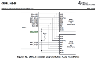
    I am not a EMIFA hardware expert, but the OMAPL138 Datasheet shows multiple NAND flash use a single EMA_WAIT pin. Can you please try to connect your second NAND device to EMA_WAIT0 to see if it works?

  • The TRM Section 20.4.2 explains the register AWCC is to configure which WAIT pin to use for which CS.