

Other Parts Discussed in Thread: TDA4VH
Is ECC (SEC/DED) testing possible on R5F internal cache memories? If yes, please provide the steps to do so.

This thread has been locked.
If you have a related question, please click the "Ask a related question" button in the top right corner. The newly created question will be automatically linked to this question.
Hi,
As per inputs from the design team, following table lists the type of R5F Cache memory and the type of error injection supported:
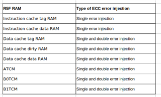
Hence there is no support for DED on I Cache. Note injection is supported by the ECC aggregator, but checking and reporting is not. This is the ARM IP limitation as there is no way to recover from DED error in the I Cache.
Following are the steps to test SEC/DED on R5F cache memories on TDA4VH:
1. Configure ECC for Cache by setting the ACTLR register to 0xE000028 in the startup.c in void __mpu_init(void) file located in sdl/test/r5f_startup prior to initializing the cache memories.
The value assigned to this register is entirely dependent on your specific use case. We do not recommend any rigid value for this register. However, considering that single bit errors are automatically corrected, it is logical to avoid aborts for correctable errors. Therefore, you may consider setting the ACTLR register to 101, which will result in an abort only for non-correctable errors.
asm("MRC p15, 0, r0, c1, c0, 0"); // Read System Control Register
asm("BIC r0, r0, #0x1 << 2"); // Disable data cache bit
asm("BIC r0, r0, #0x1 << 12"); // Disable instruction cache bit
asm("DSB");
asm("MCR p15, 0, r0, c1, c0, 0"); // Write System Control Register
asm("ISB"); // Ensures following instructions are not executed from cache
asm("MRC p15, 0, r1, c1, c0, 1"); // Read Auxiliary Control Register
asm("ORR r1, r1, #(0x5 << 3)");  //Enable ECC for Cache
asm("MCR p15, 0, r1, c1, c0, 1"); // Write Auxiliary Control Register
asm("MCR p15, 0, r0, c15, c5, 0"); // Invalidate entire data cache
asm("MCR p15, 0, r0, c7, c5, 0"); // Invalidate entire instruction cache
asm("MRC p15, 0, r0, c1, c0, 0"); // Read System Control Register
asm("ORR r0, r0, #0x1 << 2"); // Enable data cache bit
asm("ORR r0, r0, #0x1 << 12"); // Enable instruction cache bit
asm("DSB");
asm("MCR p15, 0, r0, c1, c0, 0"); // Write System Control Register
asm("ISB");
2. Enable the export functionality of R5F PMCR register for routing Cache events to ESM/ Pulsar registers.
asm("MOV R5, #0x0");
asm("MRC     P15,#0, R5, C9, C12,#0");
asm("ORR     R5, R5, #0x2");                    // Reset event counter
asm("MCR     P15,#0, R5, C9, C12,#0");
asm("MRC     P15,#0, R5, C9, C12,#0");
asm("ORR     R5, R5, #0x11");
asm("MCR     P15,#0, R5, C9, C12,#0");
asm("MOV r4, #0x60");
asm("MCR p15,#0,r4,c9,c13,#1");
3. Initialize ESM module using SDL_ESM_init() API.
4. Fill the cache by copying 32KB of data from DDR into a random array.
#define ARRAY_SIZE 32*1024 // Size of the array in bytes (32KB)
uint8_t a[ARRAY_SIZE];
uint8_t b[ARRAY_SIZE];
for(uint32_t iii=0;iii<ARRAY_SIZE;iii++)
{
a[iii]=(iii%256)+1;
}
5. Perform error injection in the R5F core.
a. For single bit error injection:
uint32_t *ptr2=(uint32_t *)0x40080008; //Set RAM ID
*ptr2=0x8;
uint32_t *ptr3=(uint32_t *)0x40080014; // ECC Ctrl Reg
*ptr3=0x28;// 0x28 for Data RAM IDs, 0x68 for Tag RAM IDs
asm("NOP"); //Enable ECC for Cache memories, Inject error into RAM ID 8
b. For double bit error injection:
uint32_t *ptr2=(uint32_t *)0x40080008; //Set RAM ID
*ptr2=0x8;
uint32_t *ptr4=(uint32_t *)0x4008001C; //ECC Error Control2 reg
*ptr4=0x30002;
uint32_t *ptr3=(uint32_t *)0x40080014; // ECC Ctrl Reg
*ptr3=0x70;// 0x30 for Data RAM IDs, 0x70 for Tag RAM IDs
asm("NOP"); //Enable ECC for Cache memories, Inject error into RAM ID 8
6. Access the cache memory region to trigger error
for(uint32_t i=0;i<ARRAY_SIZE;i++)
{
b[i]=a[i];
}
For any IP/module like R5F that has inject-only endpoints(like TCM and Cache memories), error reporting is not through the ECC aggregator but via the IP/module itself. In this case, through an error notification from R5F itself that triggers it’s own ESM event.
To verify the error injection, the following ESM events can be monitored in the ESM_STS_j Register (Offset = 420h + formula, (base address 0x40800400) :
#define SDLR_MCU_ESM0_ESM_LVL_EVENT_MCU_R5FSS0_COMMON0_ECC_SE_TO_ESM_0_0 (50U)
#define SDLR_MCU_ESM0_ESM_LVL_EVENT_MCU_R5FSS0_COMMON0_ECC_DE_TO_ESM_0_0 (51U)
The above mentioned ESM error events can be enabled in the esm_init to receive a callback incase an error is detected.
Regards,
Josiitaa
