This thread has been locked.

If you have a related question, please click the "Ask a related question" button in the top right corner. The newly created question will be automatically linked to this question.

TDA4AH-Q1: DDR CLK Certification

Part Number: TDA4AH-Q1
Other Parts Discussed in Thread: J784S4XEVM

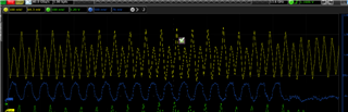
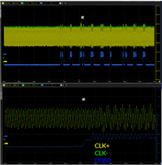
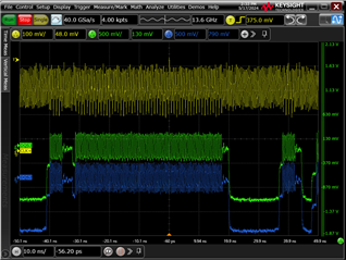
While testing the DDR CLK on our custom board to meet JDEC compliance there are failures whenever data is being transferred. As can be seen on the scope captures, whenever there is activity on the DQS line the single ended clock lines get affected. This is causing the single ended clock certification tests to fail. At first we thought it may have been power delivery related but after measuring the 1V1 line on the decoupling caps of both the processor and DDR IC there is no ripple seen. It also appears as if it could be cross talk but the only adjacent lines to the CLK in our layout are address lines and it does not appear to be coming from those. We tried to follow the EVM (J784S4XEVM) layout and decoupling scheme as much as possible and also referenced the the layout guidelines found here www.ti.com/.../spracn9e.pdf

Is there any other reasons the clock lines may be behaving like this or are there any other designs that have experienced this behavior?

  • Chris, is the memory interface functional or are you also observing read/write errors in addition to the clock cert test failures?

  • The interface is functional, we have not experienced any read/write errors yet

  • Is the noise present on all the different DDR interfaces, or specific to one?  Is the noise specific to a DQS pair?  What layers are the signals routed on and what layers are GND planes (assuming you have solid GND planes)?  What via types are used (micro-vias or drill vias)?

  • We only have an interposer on the DDRSS0 interface and not the DDRSS1 interface, so we have not been able to look at DDRSS1. The DQS pairs toggle at the same time as shown in the picture so I cant say if it is specific to one pair. Our stack up and routing is as below. We are using a 4-6-4 stack up so a combination of both types of vias are used. Via stubs are kept within the LPDDR4 layout spec limit.

    Top

    L2 -> Ground Plane

    L3 

    L4 -> Ground Plane

    L5 -> Ground Plane

    L6 -> CLK and Control routing

    L7 -> 1V1 plane 

    L8 -> Ground Plane

    L9 -> Ground Plane 

    L10  -> Bytes 0 and 2 routing

    L11 -> Ground Plane 

    L12 -> Bytes 1 and 3 routing & CLK/Control signals T-Branch

    L13 -> Ground Plane 

    L14 -> DDR IC

  • Based on Processor and Memory ball placement, I'm not sure its signal cross-talk.  CK_C is a diagonal of DQS1_P, but not near each other on memory package.  Have you done any memory pattern testing to see if the noise gets better/worse with single bit change vs entire word change?  I wonder if might be a grounding issue.  When using HDI technologies - sometimes the number of GND vias is reduced.

  • We are using the memtester application in Linux to create the activity. It does seem certain patterns such as Solid Bits and Bit Flip do create more of the noise. Others such as Random Value and Block Sequential do not seem to be as bad. I have not looked into what each of the tests are actually sending yet. There are opportunities in our layout to improve grounding that we plan on implementing on our next pass but mostly it is just extending an already existing ground via to connect on more layers.

  • If bit patterns with larger number of bits changing is creating more noise - could indicate SSO noise issue.  This is usually from high impedance on power or ground planes.  From previous post, processor and memory on BOT of PCB.  Likely decoupling on TOP PCB.  All decoupling current/return must go through the PCB (Vias).  I have see HDI board use lots of vias to closes GND plane (layer 13 in this case), but have limited vias to opposite side of PCB - where all the decoupling is located.  This can make decoupling caps very ineffective.