
- Ask a related questionWhat is a related question?A related question is a question created from another question. When the related question is created, it will be automatically linked to the original question.

Tool/software:
Hello TI exprits,
In the BYD SA5 we meet a very strange issue,we configurated the main domain MSRam,
in the previous tikets we have mentioned that.
and we put some text section in the 0x80000 which we congfigured in the RAT function
but currently we do some stress test and found that,some times when the sbl to copy the data from scratch memory to the main domain msram
some of the text is not correct which load in the main domain MSARAM,but the text in the DDR and mcu msam is all correct.
such as the text in the 0x81fb4 should be
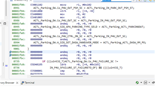
which the correct data is like bellows
and I read the memory directly and found that there are 32bytes from 0x81fa0 to 0x81fbc which have been change to 0,

and we also check the text in the main domain MSRAM,
there are many place which have been changed
such as here
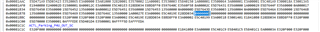
such as here

such as here

and all changed is 32 bytes which should be text code but was change to 0,is there any cache issue or dma issue?
can we use the main domain SRAM for the mcu text code.Could you pls check is this methods which use main domain MSRAM in mcu domain is fine,can you check this with your IP design TEAM for this.


