AM6442: Simulation result

Part Number: AM6442

Tool/software:

Hi Support Team,

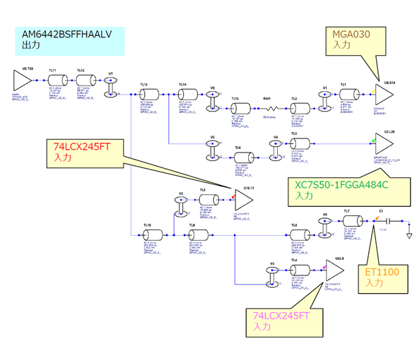
Our customer, who is doing SI Simulation, has the following question about GPMC I/F.
The waveform is not a square wave, due to the small drive strength of the IBIS model (AM64x SR2.0 BSDL Model).

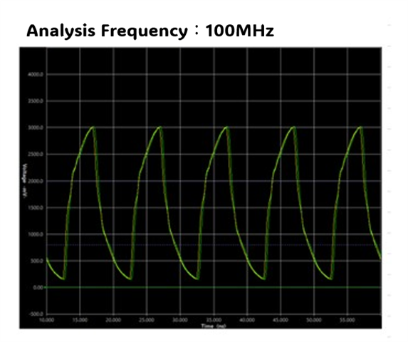
The simulation is still in progress, but I wonder if the current result is correct.
If not, please let me know how to fix it.

Best Regards,
Kanae

  • Hello Kanae

    Thank you for the query.

    Can you please provide additional details on the simulation setup and connections.

    Regards,

    Sreenivasa

  • Hi Sreenivasa,

    Thank you for your support.

    Here are Model and  Setup on this Simulation.

    sprm810.ibs
    AM64:lvcmos1_nom_3p3_h

    spartan7.ibs
    SPARTAN7:LVCMOS33_F_12_HR

    Please refer the attached PDF file for the connection and other details.

    Simulation.pdf

    If you need other information, Please let me know.

    Best Regards,
    Kanae

  • Hello Kanae

    Thank you.

    The values in the PDF are not readable.

    Regards,

    Sreenivasa

  • Hi Sreenivasa,

    Thank you to point it out.

    Here is an enlarged topology image in Page-1 and Page-3.
    Please let me know if there are any other values you need to confirm.

    Please refer to the PDF for the parts that are not translated into English.

    Best Regards,
    Kanae

  • Hello Kanae, 

    Thank you.

    Let me check with the simulation expert.

    Regards,

    Sreenivasa

  • Hi Sreenivasa,

    Thank you for your support.
    Our customer has requested answer to the following questions by the end of this week (Japan time).

    1. Is the capability of the provided IBIS model appropriate for the above waveforms?

    2. As mentioned in the following thread, the drive strength of AM6442 cannot be changed by registers,
     so is it necessary to add a transceiver or other measures to achieve a square wave?

    https://e2e.ti.com/support/processors-group/processors/f/processors-forum/1296235/am6442-lvcmos-drive-strength

    Best Regards,
    Kanae

  • Hello Kanae,

    Thank you for the inputs.

    Let me check with the team but i suspect if i would have some inputs by end of this week.

    Regards,

    Sreenivasa

  • Hi Sreenivasa,

    Thank you for your reply.

    My apologies for the short deadline for a response, but if you are unable to respond this weekend,
    please let me know as I need to report back to the customer when I can expect to hear back from you.

    Best Regards,
    Kanae

  • Hello Kanae,

    Thank you.

    I have reached out to the expert to review.

    I will update you with his inputs as i receive.

    Regards,

    Sreenivasa

  • Hello Kanae,

    Please note the inputs from our simulation expert Shriram

    1. There are multiple endpoints connected to the output driver from the AM6442 SoC. This is not recommended. Point-to-point connection is recommended. Each endpoint except the last one will suffer from the mid-supply “step” in the waveform that is introduced due to being some distance away from the end of the T-line.
    2. Presence of stubs in the layout due to multiple connections will cause additional reflections which will further degrade signal integrity
    3. As noted, shorter wiring length will result in better signal integrity. A possible topology that could be explored is to mount FPGA at the bottom of the board directly beneath the SoC (assuming SoC is mounted on the top side)
    4. Please check to see if there is excessive power supply noise in the system. If the board-level PDN is not robust enough it will cause additional supply noise that will further degrade signal integrity. Improving the PDN will also improve signal integrity.

     Regards,'

    Sreenivasa

  • Hi Sreenivasa,

    Thank you for your support!
    I will share this with my customer.

    Best Regards,
    Kanae

  • Hello Kanae,

    Thank you for the note.

    Regards,

    Sreenivasa

  • Hi Sreenivasa,

    Thank you for your support!
    Here are additional questions from our customer.


    Regarding the answer to 1. 2. above.
    Although EVMs are also designed to connect to multiple endpoints,
    we think the answer is unrealistic. After all, we take it to mean that
    only one device is supposed to be connected, but what is the drive current in mA?


    Regarding the answer to 3. above.
    Since the Pitch and placement of the pads are different,
    you are forcing us to adopt interstitial via, which is not a realistic measure
    since it is very costly for IVH boards.
    We think that the current bus configuration and layout is the best (CPU, FPGA, buffer)
    when considering the reuse of board patterns for other models.
    We are considering setting the fastest bus timing including margin during debugging.

    Can we proceed with the board design assuming that the current waveform
    with low CPU drive capability is accepted as true?

    Best Regards,
    Kanae

  • Hello Kanae,

    Thank you for the inputs.

    Let me review the inputs and check internally.

    Regards,

    Sreenivasa

  • Hi Sreenivasa,

    Thank you for your support.

    Could you please confirm the progress of this request and the expected date of response,
    as I need to report back to the customer when you can reply to me.

    Best Regards,
    Kanae

  • Hi Sreenivasa,

    Do you have any updates on this?

    Best regards,

    Mari Tsunoda

  • Hello Kanae,

    Thank you for checking.

    The Simulation expert is on vacation and expected to be back Tuesday Dallas time.

    I will follow-up and update you.

    Regards,

    Sreenivasa

  • Hello Kanae,

    Regarding the answer to 1. 2. above.
    Although EVMs are also designed to connect to multiple endpoints,
    we think the answer is unrealistic. After all, we take it to mean that
    only one device is supposed to be connected, but what is the drive current in mA?

    We do not define output current drive.  The customer will need to use the IBIS model in a simulation to determine output performance and the resulting signal integrity with their specific PCB implementation.

    Regards,

    Sreenivasa

  • Hi Sreenivasa,

    Thank you for your reply.
    Is the following understanding correct?

    ・The IBIS model provided by TI outputs a waveform with low CPU drive capability,
     but this waveform is “true” for the current usage.
    ・The user needs to determine the output performance and resulting signal integrity of
     the actual board design (specific PCB implementation) using the IBIS model in simulation
     of this low driving capability.

    Best Regards,
    Kanae

  • Hello Kanae,

    Thank you. 


    The IBIS model provided by TI outputs a waveform with low CPU drive capability,
     but this waveform is “true” for the current usage.

    The drive strength currently supported by the AM64x device is correctly represented in the IBIS model.

    The user needs to determine the output performance and resulting signal integrity of
     the actual board design (specific PCB implementation) using the IBIS model in simulation
     of this low driving capability.

    This is  correct.

    Customer must simulate their design using PCB extractions and the IBIS models of each device, and apply their own judgement based on their simulation results.

    Regards,

    Sreenivasa

  • Hi Sreenivasa,

    Thank you for your support.

    I will share it with my customer.

    Best Regards,
    Kanae

  • Hello Kanae,

    Thank you. 

    I am working on the other question.

    Regards,

    Sreenivasa

  • Hello Kanae,

    Additional inputs

    Regarding the answer to 3. above.
    Since the Pitch and placement of the pads are different,
    you are forcing us to adopt interstitial via, which is not a realistic measure
    since it is very costly for IVH boards.
    We think that the current bus configuration and layout is the best (CPU, FPGA, buffer)
    when considering the reuse of board patterns for other models.
    We are considering setting the fastest bus timing including margin during debugging.

    Can we proceed with the board design assuming that the current waveform
    with low CPU drive capability is accepted as true?

    We only use PTH vias on all our EVMs. Blind/buried vias will add cost due to extra lamination cycles.
    The BGA pitch is 0.8mm so there should not be any need to use via-in-pad, if that is what they mean.
    The bottom placement was only a suggestion as it might help with signal integrity.
    The root cause of their issues is that they are connecting 5 devices to a single output buffer.
    With a 60 ohm drive strength and reflections from the stubs/branches, it is not surprising that the waveforms are as bad as they are noticing.
    Ultimately, it is their decision on how to determine the best topology of their board.

    To answer their specific question, customer can proceed with the design and simulations
    TI will never tell a customer their PCB design is good enough.
    Customer must simulate their design using PCB extractions and the IBIS models of each device, and apply their own judgement
    based on their simulation results.

    The drive strength currently supported by the AM64x device is correctly represented in the IBIS model.
    The design/apps team is internally looking into improving the drive capability. I do not have any additional information to share currently.

    Regards,

    Sreenivasa

  • Hi Sreenivasa,

    Thank you for your support.

    Referring to the above response, our customer plans to make adjustments to
    the custom board and complete the simulation.
    After completing the simulation, the customer provided the following feedback,
    Do you have any plans to improve the following?
    If so, when?
    If no, please explain why you do not think it is necessary to make any improvements.

    ***Feedback from customer***
    [ AM6442 ]
     -It is difficult when connecting multiple devices because GPMC recommends point-to-point connection.
     The notes for using multiple devices are not described in the technical documentation.
     -The drive capability is not specified and is weak, which makes it very difficult to use as a device.

    [IBIS model]
    The IBIS model is not a good reference (simulation) for design because of the difference from actual devices.


    Also, regarding the following comments, when will you share with the users what is being studied
    by the design/application team to improve the drive capability?

    Sreenivasa said;.
    The design/apps team is internally looking into improving the drive capability.
    I do not have any additional information to share currently.


    Best regards,
    Kanae

  • Hello Kanae,

    Thank you.

    Also, regarding the following comments, when will you share with the users what is being studied
    by the design/application team to improve the drive capability?

    Sreenivasa said;.
    The design/apps team is internally looking into improving the drive capability.
    I do not have any additional information to share currently.

    I do not have a timeline to share.

    I am looking into other inputs.

    Regards,

    Sreenivasa

  • Hi Sreenivasa,

    Thank you for your support.
    Please continue to look into this issue.
    Please let me know when you can expect to hear back from the Product Division.

    Best Regards,
    Kanae

  • Hello Kanae,

    Thank you.

    Will follow-up and update.

    Regards,

    Sreenivasa

  • Hi Sreenivasa,

    Please let me know when you can expect to hear back from the Product Division.

    Best Regards,
    Kanae

  • Hello Kanae,

    Thank you.

    Will follow-up and update.

    Regards,

    Sreenivasa