[FAQ] AM64x (AM6442, AM6441, AM6422, AM6421, AM6412, AM6411) and AM234x (AM2434, AM2432, AM2431 - ALV): Custom board hardware design - SK and EVM EXT_REFCLK1 CLKOUT0 use case and configuration

Part Number: AM6422
Other Parts Discussed in Thread: SK-AM64B, , CDCLVC1310, TUSB4020BI, SYSCONFIG, AM2434

Tool/software:

Hi,

In AM6422 evaluation board SK-AM64B. It connect the EXT_REFCLK1 to CLKOUT0 signal. i have some question about it.

1. EXT_REFCLK1 is 3.3V. Why it connect to a 1.8V clock buffer. Will it damage the buffer?

2. If EXT_REFCLK1 output the signal to 1.8V buffer. How the clock generate from EXT_REFCLK1. looks like the buffer also support the main domain clock input. if the main domain doesn't has the input clock firstly, how the EXT_REFCLK1 generate clock signal. if I am wrong, how the circuit work?

 the PROC101D evaluation board has similar questions. looks like logic level is not same. And if the buffer CDCLVC1310 input is select to primary. how the main/mcu domain clock work firstly.

Best Regards,
Shu  

  • Hello Shu  

    Thank you for the query.

    Please refer below.

    1. EXT_REFCLK1 is 3.3V. Why it connect to a 1.8V clock buffer. Will it damage the buffer?

    Supply voltage: 3.3 V, 2.5 V, or 1.8 V – 3.3-V tolerant input at all supply voltages – Fail-safe inputs

    In AM6422 evaluation board SK-AM64B. It connect the EXT_REFCLK1 to CLKOUT0 signal. i have some question about it.

    1. EXT_REFCLK1 is 3.3V. Why it connect to a 1.8V clock buffer. Will it damage the buffer?

    2. If EXT_REFCLK1 output the signal to 1.8V buffer. How the clock generate from EXT_REFCLK1. looks like the buffer also support the main domain clock input. if the main domain doesn't has the input clock firstly, how the EXT_REFCLK1 generate clock signal. if I am wrong, how the circuit work?

    This is used when the SOC had the crystal clock option configured.

    I am not sure if this has been tested.

    I need to check and comeback.

    Regards,

    Sreenivasa

  • Hello Shu  

    Please refer below. The same pin can be configured as Clkout0. The EVM configuration is a valid configuration that can be used when the SOC is configured for Crystal.

    6.3.22.3 System
    6.3.22.3.1 MAIN Domain

    CLKOUT0
    O
    RMII Clock Output (50 MHz). This pin is used for clock
    source to the external PHY and must be routed back to
    the RMII_REF_CLK pin for proper device operation. A19, U13

    EXT_REFCLK1
    I
    External clock input to Main Domain, routed to Timer
    clock muxes as one of the selectable input clock
    sources for Timer/WDT modules, or as reference clock
    to MAIN_PLL2 (PER1 PLL) A19

    Regards,

    Sreenivasa

  • Hi Sreenivasa,

    That is my concern. looks like the EVM make the EXT_REFCLK1 to a clkout0 function, it is a output clock to a clock input buffer. the buffer is connected to SoC main clock input. So where is the first clock come from? if the SoC clock from a crystal, where the EXT_REFCLK1 clock go. In EVM, it go to same buffer input as the crystal. I don't think the buffer can use two inputs at same time.

    Best Regards,

    Shu

  • Hello Shu, 

    The SOC CLKOUT0 can be used only to clock the EPHY and can only be used when a crystal is connected to the SOC oscillator.

    Regards,

    Sreenivasa

  • okay, that make sense. 

    thank you very much

  • Hello Shu, 

    Thank you for the note. The explanation is valid for AM64x as well as AM62x, AM62Ax and AM62Px SKs.

    Regards,

    Sreenivasa

  • Ai All, 

    Additional inputs on usage of clock and buffers.

    When an external clock (LVCMOS) oscillator is used as the clock source for the processor and the EPHY, a single oscillator could be used for the processor and the EPHY or separate oscillator can be used. When using a single oscillator, the clock output is recommended to be buffered before connecting to processor and EPHYs.
    Single output, individual buffer ICs for processor and EPHY(s) or Dual or Multiple output buffer IC for processor and EPHY(s) can be used to connect the clock output from the oscillator to the processor and the EPHY(s)
    For specific use case (requirement for some of the industrial applications using Time Sensitive Networking (TSN)), two or more output (based on number of EPHYs used) buffer with a single input is recommended for the processor and the EPHY(s).

    Regards,

    Sreenivasa

  • Hi Board Designers,

    Inputs related to clock performance

    Customer would like to know if he can use the CLKOUT0 to supply the TUSB4020BI (24MHz, ±100PPM or better frequency stability and <50ps absolute peak-to-peak jitter). 

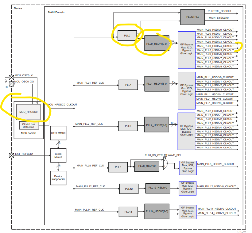
    CLKOUT0 being sourced from MAIN_PLL0_HSDIV4_CLKOUT I'd like to get the specifications of the internal circuitry (MCU_HFOSC0, PLL0 , PLL0_HSDIV) in order to know if the signal is compliant to the input clock requirements of the TUSB4020BI . 

    Thank you, 

    Geoffrey


    image.png

    The CLKOUT0 is only a 25 or 50MHz clock intended to be used for Ethernet PHYs.  More information can be found.
    We also do not define performance of the clock output because it can be system dependent. You should validate the clock output performance meets the clock input requirements for the attached device across all operating conditions before deciding to use it.

    The answer to this question depends on your product requirements. I have been told some of our customers using the PRU_ICSSG subsystem in AM64x may need a common clock source to all Ethernet PHYs when implementing a Time-Sensitivity Network. The common clock source eliminates PPM error differences associated with multiple reference clock sources. You will need to research your product requirements and understand how to implement the appropriate clocking topology to achieve the requirement.

    2. No. The CLKOUT0 signal function can only be configured to source a 25MHz or 50MHz clock. The intended function of this clock output was to be used with an Ethernet PHY, where it can be configured to source a 50MHz clock for the RMII peripheral, or a 25MHz clock in lieu of a crystal circuit. I suggest you use the clock tree tool that is part of the SYSCONFIG tool to understand the internal clocking topology of AM64x devices.

    3. The CLKOUT0 signal function is not selected by default. Software must configure the appropriate multiplexers in the signal path to select either 25MHz or 50MHz, configure the respective PADCONFIG register to select the CLKOUT0 signal function, and enable the output buffer associated with the pin being used for this signal function. Note: The internal multiplexers and pin multiplexing logic which selects and enables the signal function may create a short clock pulse (glitch) since the registers which control these operations are not synchronous to the clock signal. This means the device you are source with this clock should be held in reset until software has initialized the entire signal path and the clock is stable. We also do not define performance of the clock output because it can be system dependent. You should validate the clock output performance meets the clock input requirements for the attached device across all operating conditions before deciding to use it

     RE: AM625: LVCMOS Digital Clock Source 

    It is very difficult for TI to select a firm limit for this parameter since there are many system-level contributors like power supply noise and specific PLL configuration that influence device performance. Therefore, we recommend customers validate their system across the full range of expected operating conditions for any reference clock solution.

    Regards,

    Sreenivasa

    Regards,

    Sreenivasa

  • Hi Board Designers,

    Inputs related to OBSCLK0

     AM2434: Using OBSCLK0 or MCU_OBSCLK0 to generate FPGA clock 

    The customer wants more information why he cannot use the OBSCLK0 and the MCU_OBSCLK0 pins of the AM2434 to generate a clock signal for his FPGA.
    I told him that these pins are for observation only, but he wants to know what are the limitations for using the signals and what will happen if they use them.
    Could you please help me with an additional information?
    There is a good chance these clock outputs will produce a short cycle when the clock signal function is initially selected via the AM243x pin multiplexing logic because the signal function selection is not synchronized with these clocks. The AM243x signal functions change asynchronous to these clocks. This could be a problem for any synchronous logic being clocked from these outputs. They should consider holding any logic being sourced by these outputs in reset until the clock signal function is selecting and producing full cycles.

    These outputs are defined as “observation only” because they were not designed to meet any specific clock performance. Therefore, TI has no plans to define any performance parameters associated with these outputs. A customer may find they provide a clock output that is good enough for their system design, but any effort of validating the outputs meet their requirements is their responsibility. TI doesn’t plan to assist with any effort required to use these clock outputs in a customer’s system design.

    Regards,

    Sreenivasa