Other Parts Discussed in Thread: TPS6594-Q1, TPS65224, AM62A7-Q1, TPS6593-Q1, TPS22918, AM62A7
Tool/software:
HI Board designers,
I am designing my board using TPS6593 PMIC
Are there some common recommendation or observations that i should be aware?

Tool/software:
HI Board designers,
I am designing my board using TPS6593 PMIC
Are there some common recommendation or observations that i should be aware?
HI Board designers,
Refer below, FAQs, common queries and replies
If you are using the SK-AM62A-LP EVM with the TPS65931211-Q1 PMIC, then you can modify the hardware to change the default voltage on VDD_CORE which is supplied by the PMIC multi-phase Buck1/2/3.
The GPIO6 of the PMIC was configured to set the voltage on Buck1/2/3 with the following polarity:
During power up, the PFSM for the '1211 reads the state of GPIO6 10ms after it has enabled the 3.3V load switch. If GPIO6 is pulled up to that signal, BUCK123 will be 0.85V.
Therefore, from the PMIC perspective Pull GPIO6 HIGH to the 3.3V load switch signal
This information along with all the PMIC NVM configuration was documented in the following user's guide: https://www.ti.com/lit/pdf/slvucm3
Regards,
Sreenivasa

HI Board designers,
Refer below, FAQ
The full PMIC orderable part number is TPS65931211RWERQ1 and it comes pre-programmed to meet the voltages and sequence requirements of the AM62A procesosr. This part number can be found on table 2-1 of the document you referenced in the message
[FAQ] TPS6594-Q1: Residual Voltage Check
Regards,
Sreenivasa
HI Board designers,
Using TPS65224 for AM62A
Refer below, FAQ
Additional inputs
We get request from schematic review team to add a buffer between PMIC TPS65224 RSTOUT pin and SOC MCU_PORZ pin.
I think the reason is that the SOC MCU_PORZ will require the rising edge and falling edge. So would you like to share the detail.
Such as the rising edge slew rate, rising time and so on required by MCU_PORZ as input?
The PMIC nRSTOUT is a open drain slow ramp output from the PMIC.
When a slow ramp reset input is applies to the MCU_PORz there are likely chances that the internal reset circuit could glitch.
A discrete push pull output buffer is recommended to minimze the slew.
We do not have a spec for the MCU_PORz. The recommendation is faster the better. (<10ns)
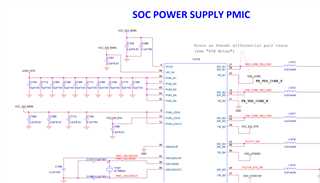
if possible, could you help me confirm the timing relationship for Buck1 (VDD_CORE) and LDO0 (VDDR_CORE)
In the startup sequence the buck1 goes high at 5.9 ms and LDO3 (VDDR_CORE) at 6.45 ms. In the shutdown LDO3 goes down at 0.5 ms and buck 1 at 1 ms. Timings are measured from the enable rising/falling edge.
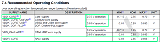
Partial IO - What about VDD_CANUART (core supply)?
For Partial IO, VDDSHV_CANUART (1.8V/3.3V) and VDD_CANUART (0.75V/0.85V) are both connected to always-ON rails. When Partial IO mode is not use, the CANUART supplies are connected to the same rails as the remaining IOs and CORE.
Regards,
Sreenivasa
Hi Board designers
Input regarding selection of PMIC:
The recommend PMIC(s) on the product folder or used on the SK or EVM schematics has been designed considering the power sequencing, supply rail output slew, nRSTOUT (reset output) delay output from PMIC connected to MCU_PORz after all the supplies ramp for clock to be stable and the sizing of the supply rails based on the processor worst case current draw.
When choosing an alternate non-TI PMIC, the recommendation for custom board designers is to review the relevant collaterals including the data sheet and Maximum Current Ratings document and follow the requirements/recommendations. The recommendation is to review the slew rate requirements, Power-up and power-down sequence sections of the data sheet and confirm the non-TI PMIC based power architecture follows the recommendation.
An important point to note is the processor does not support dynamic scaling of the core voltage or the analog supplies.
Inputs regarding supply decay
Refer below FAQ
I have placed the note in both sections because it applies to both power-up and power-down. The power-up sequence should not begin until all power rails are below 300mV, and the power-down sequence is not complete until all power rails are below 300mV.
Regards,
Sreenivasa
HI Board designers,
Inputs on power supply sizing:
Using Maximum Current Ratings application note vs Power Estimation Tool PET
The max current app note is representing the current draw for a group of rails. Please note that it is not expected for this current to necessarily be replicated in the power estimation tool. The PET will tend to show more average use case power while the max current app note is intended to be used for power supply sizing as it will allow for the max transient on these groups with some margin. The PET should not be used for power supply sizing.
Power Estimation Tool (PET) and the max current rating apps note serve two different purposes. The PET is used to estimate active power consumption for a specific use case/application. The max current rating apps note can be used for supply sizing when designing a custom power solution
Regards,
Sreenivasa
HI Board designers,
Note:
How were these pdn specs derived? Is it based on worst case analysis?
Yes it is based on worst case load transient estimates for a given SoC design.
The Target impedance for AM62x and AM62xSiP will be identical as the same worst case load transients exist on both designs since they share the same die.
Via sharing recommendations in the escape application note are only made to help guide a customer to escape the design with fewer vias in the VCA regions. The number of vias used for escaping signals will ultimately depend on the specific customer use-case, the number of interfaces that need to be implemented and the layer count. If the specific use case allows the customer to use more vias for VDD_CORE in the VCA regions, that is definitely a valid approach. Per-pin loop inductance guidelines are more applicable for single-pin supplies that are connected to a decap. In case of multi-pin supplies like VDD_CORE where there are a number of parallel connections to multiple pins/decap thru multiple vias, it is hard to tie it back in to a per-pin requirement. The most important target to meet is the impedance target specified in Table 7-6 of the PDN Applications note. This table is the same for AM62x and AM62x SiP.
We do not include Buck output inductance in PDN simulations.
For VDDS_DDR: we do not recommend using target impedance as the signoff for DDR.
Refer to the AM62x, AM62Lx DDR Board Design and Layout Guidelines which outlines all details of power aware SI/PI simulations
that need to be run. The eye mask checks from these power aware simulations are the signoff.
Power Distribution Networks: Implementation and Analysis
Sitara Processor Power Distribution Networks: Implementation and Analysis
https://www.ti.com/lit/pdf/sprac76
Note: The decoupling capacitor numbers and type on the SK/EVM are only intended to serve as a guideline for customers. The true pass/fail criteria is the target impedance published in the PDN app note.
High Speed Board design and Signal integrity simulation
https://www.ti.com/lit/pdf/spraar7
https://www.ti.com/lit/pdf/spracn9
https://www.ti.com/lit/pdf/sprabi1
Inputs on PDN
Please refer below inputs i received:
Please note these are only recommendations and they need to contact their EDA vendor on what works best for their specific simulation environment.
1、Do I need to separate VDD_CORE-1 to 17 for simulation, or use VDD_CORE as a Port?
TI>> You can lump all VDD_CORE BGAs together as a single terminal for the port
2、Do I need to include the PMIC FB loop in the simulation?
TI>> If you are simulating only for AC impedance (target impedance checks) this is not required. The board layout from the inductor onwards (inductor not included) can be modeled and PMIC FB loop can be studied separately.
3、 Is the simulation starting frequency from 1Hz or from a minimum of 100kHz for the capacitor S2P?
TI>> There should be some DC frequency points added. Please check with your EDA vendor on the exact setup and simulation points needed to generate causal models.
I added additional inputs related to PDN and decoupling capacitors for reference.
The voltage at the device ball must never be below the MIN voltage or above the MAX voltage for any amount of time. This requirement includes dynamic voltage events such as AC ripple, voltage transients, voltage dips, and so forth
PCB design & Dcap scheme combine to form your board's Power Distribution Network (PDN) that should meet recommended SoC PI performance targets for robust processor operations. Each PCB design has a "unique finger-print" based upon component placements, power & Gnd routing, layer assignments, via qtys & locations, Dcap mounting & loop inductance, Dcap parameters, etc. As a result, an optimized Dcap scheme will vary from one PCB design to another but should provide a system PDN that meets PI performance targets when combined together. Similarly, the PI simulation tools can impact the estimated ZvsF response values, especially above 3.0MHz where non-3D extraction tools can return better Z values (10-15% less than more accurate 3D tools). This ican be due to a non-3D tool is only extracting a PCB's X & Y design elements & assuming a power & Gnd via inductances. Due to the 3D nature of current flow across & through a PCB from power & Gnd planes on different PCB layers, a 3D extraction gives a more accurate series inductance estimate needed to more accurately model power & Gnd vias which leads to a more accurate power rail impedance (ZvsF) response
it would be difficult to comment on reducing the amount of decoupling caps without going through the exercise ourselves. That said, you can likely prioritize the high-current and sensitive analog rails, then look to share bypass caps when you hit space constraints. Having decap as close to the BGA as possible will reduce inductance and improve their efficacy (two supply vias with a shared decap would be better than a decap located far away in most circumstances).
Please be aware that each PCB design is unique and may need different Dcap scheme to meet recommended PI parameter targets
Regarding decoupling capacitors, the recommendation is to start with the EVMs decoupling and then optimize (if needed) based on your power simulation results.
For the placement of the Caps and values, we would still recommend using the EVM as a reference along with the PDN document.
SK uses an EMI Filter at 1uF, can I replace it with a general ceramic capacitor?
The SK performance has been tested with 3-T terminal caps.
You may have to add multiple 2-T caps for each cap and perform simulations to finalize the values.
AM62A7-Q1: Sitara Impedance Help
These are the target impedance estimates for AM62A rails. These can be taken as the target impedance requirements for the respective rails.
We do not have target impedance estimates for the other rails.
| Voltage Rail | Freq Range | Target Impedance (mOhms) |
| VDD_CORE (0.75V) | Low (< 1MHz) | 7.0 |
| Mid (1 - 20 MHz) | 11.7 | |
| High (20 - 50 MHz) | 23.4 | |
| VDD_CORE (0.85V) | Low (< 1MHz) | 6.9 |
| Mid (1 - 20 MHz) | 11.4 | |
| High (20 - 50 MHz) | 22.9 |
We have a high confidence in the target impedance estimates from a simulation standpoint, as our own boards have been designed to these requirements.
Does VDD_CORE (0.85V) rail refer to the same VDD_CORE pins as VDD_CORE (0.75V), but with target impedance if 0.85V is supplied to VDD_CORE?
OR, does VDD_CORE (0.85V) refer to the VDDR_CORE (0.85V) supply pins?
With regards to the VDD_CORE, the target impedance should refer to the same pins with either 0.75V and 0.85V supplied. The load transients and supply noise tolerances will be slightly different for the different voltages and so the target impedances will also differ slightly.
SPRAC76G does not list VDD_DDR Target Impedance across frequency ranges, it says "For more information, see AM62Ax DDR Board Design and Layout Guidelines." But this document also does not provide VDD_DDR Target Impedance across frequency ranges (as far as I can tell).
Please provide VDD_DDR Target Impedance across frequency.
We do not recommend using VDD_DDR Target impedance across frequency as an appropriate metric for signoff, due to very low load transients. For DDR signoff, we recommend running Power-aware Signal Integrity simulations as outlined in the AM62Ax DDR Board Design and Layout Guidelines App note.
Note:
We do not include Buck output inductance in PDN simulations.
For VDDS_DDR: we do not recommend using target impedance as the signoff for DDR.
Refer to the AM62Ax, AM62Px, AM62Dx LPDDR4 Board Design and Layout Guidelines which outlines all details of power aware SI/PI simulations
that need to be run. The eye mask checks from these power aware simulations are the signoff."
For frequencies above 50 MHz the board decoupling caps do not play a critical role. SoC and Package decaps (if any) will be dominant beyond 50 MHz
PDN application note
https://www.ti.com/lit/an/sprac76g/sprac76g.pdf
Regards,
Sreenivasa
HI Board designers,
E2E links for reference
All parts we sell are already pre-programmed. Under no circumstances will you ever receive a part with no programming on it.
The TPS6593-Q1, the TPS6593 is the generic portion of the part number.
TPS6593XXXXRWERQ1, the XXXX denotes a specific programming placed onto the device, as you see on the product page all devices have the TPS6593XXXXRWERQ1 naming scheme.
Are you not able to turn on your device, if so please open another E2E ticket so we can address your concerns there rather than here as this question is for acquiring PMICs not troubling shooting, thank you.
Regards,
Sreenivasa
Hi Board designers,
Refer below input related to eFuse caps and pinout
TPS22918 5.5-V, 2-A, 52-mΩ On-Resistance Load Switch
Regards,
Sreenivasa
Hi Board designers,
FYI only (can be used as reference)
A few important points...
The fact you are seeing these particular interrupts, you should double check your schematic and layout out for two things:
Early versions of TDA4 SKs and EVMs had small mistakes on the above two points. Boards powered up and were functional but some saw subpar stability on stability on buck performance.
Regards,
Sreenivasa
Hi Board designers,
FYI on board bring-up PMIC related
(+) AM62A7-Q1: AM62A7 SoM not powering ON - Processors forum - Processors - TI E2E support forums
FB_B3 cannot be left floating. As note in the PMIC user's guide: "FB_B3 must be connected to 3.3 V. If 3.3 V is not connected to FB_B3 when the monitor is enabled then the device goes to the hardware SAFE RECOVERY state, and the processor voltages are disabled".
(+) AM62A7: AM62A7 power TIMING - Processors forum - Processors - TI E2E support forums
The sequence requirements between VDD_CORE and VDDR_CORE must be followed during the power-up sequence. This is a hard requirement.
For power down, we strongly recommend to discharge VDDR_CORE below ~300mV before turning-OFF the next rail in sequence (VDD_CORE). However, we don't have any data that would indicate an issue if VDD_CORE discharges faster than VDDR_CORE during power-down. This power-down requirement is included in the spec because having a potential on VDDR_CORE greater than VDD_CORE + 0.18V during power-down is not fully validated/characterized.
Regards,
Sreenivasa
Hi Board designers,
Additional inputs:
If the software is running just before the SoC is powered off, will it be affected the next time it is started up?(From a hardware perspective)
Triggering a power-down sequence before finishing the software-OFF process is an unknown state for the SoC where the expected behavior is not defined. There could be a risk of data corruption if there is a power supply change during the software off process. This is one of the reasons we recommend following the documented power down sequence and make sure the software-OFF request is complete before turning-OFF the supplies.
Regards,
Sreenivasa
Hi Board Designers,
Inputs related to 3-terminal caps
For TDA4AL PMIC reference design schematic, why we need use 4*three-terminal capacitance? If we don't use, what is the risk?

The 3-terminal capacitors are more effective at filtering high frequencies than a 2-terminal equivalent, as the equivalent series inductance is lower. If you choose to replace these capacitors, you may see more higher frequency noise.
This excerpt from the Buck Output Capacitors subsection of the Application and Implementation chapter in the TPS6594-Q1 datasheet shows that the 3-terminal capacitors are recommended.
There are also 3-terminal in the input of the buck, why we also need add them in the input? Thanks!
Thanks for the clarification. I now see the capacitors in your question are each connected to one of the BUCK inputs 1-4. The 3-terminal capacitors were used here due to the PVIN also being a noisy signal that benefits from a low inductance capacitor. Looking at the Layout Guidelines in the TPS6594-Q1 datasheet, we can find that the most important parameter of the decoupling capacitors on PVIN_Bn is the inductance.

These capacitors are helpful to minimize the effect of the BUCKs switching at 2.2 MHz or 4.4 MHz on the VCCA rail. These provide capacitance at a lower inductance that is more capable of managing the high frequency current switching. PVIN_B5 does not have one of these 3-terminal capacitors due to the relatively low current draw of BUCK5.
Regards,
Sreenivasa
Hi Board Designers,
Inputs related to 5V operation
You can use the PMIC Efficiency Estimator Tool (PEET) https://www.ti.com/tool/PEET-GUI to do this - select TPS6594-Q1 in the tool. The efficiency is same between the two devices.
PMIC VPP Current
t500mA is enough. Note: The 1.8V source for VPP should have an internal active discharge function that gets turned on when the source is disable to ensure VPP is held to 0V during normal operation.
TPS65931211-Q1 PMIC User Guide for AM62A
Using 5V Input Supply
The PDN described in this user's guide was designed for 3.3V input supply. However the TPS65931211-Q1
NVM also supports 5V input supply. The default NVM settings on TPS65931211-Q1 have the UV/OV disabled on
VCCA so PMIC can use either voltage (3.3V or 5V). If 5V supply is used, then a 3.3V discrete Buck is required
for the 3.3V IO domain instead of a power switch. The external 3.3V Buck can be enabled by GPIO4 and needs
to ramp from 0V to 3.3V within the 10ms delay that was assigned to GPIO4 in the any2active sequence.
LDO1 is configured as “bypass” and requires a 3.3V supply. This LDO can be supplied by the output of the
discrete 3.3V regulator. TI also recommends supplying the remaining LDOs (LDO3 and LDO4) with the discrete
3.3V regulator to reduce power dissipation. VIO_IN must be supplied by 3.3V as well.
When using 5V instead of 3.3V, the voltage from the pre-regulator cannot be directly connected to
VDDSHV_CANUART. In this case, VDDSHV_CANUART can be supplied by the same discrete 3.3 V Buck
1.Whether PVIN_Bx can be connected to 5V and other power(VCCA, VIO_IN, PVIN_LDOx ) are all connected to 3.3V, please double check again?

The recommended is have the PVIN_LDOx not to exceed the VCCA input voltage supply

The recommendation is not use the PVIN_Bx at 5V if the VCCA is 3V3.
2. And if they can, Is there any special used guide for this PMIC within our used case
The User's Guide for the TPS65931211, which I'm sure you are aware of talks about changing the input voltage of the system from 3V3 to 5V.
In section 3.1.2, link to guide here
Is there any suggestions from ur side? The SCH is shown below.
PS, attached the PMIC SCH design in our project as below, which also be reviewed by TI.
I remember this one, my apologies, the understanding was that the input supply from VCCA, PVIN_Bx, & PVIN_LDOx would all be switched over to 5V, not just a select few.
If they have a choice between using 5V input on the previously mentioned pins of VCCA, PVIN_Bx, & PVIN_LDOx or 3V3, using 3V3 they need to pick one and use all three of these inputs, please have them review section 3.1.2 in the User's guide
AM62A7: Kernel Panic Occurs During Operation
We have identified the root cause and resolved the issue.
The problem was related to the VCC_CORE voltage.
According to our board’s hardware design, VCC_CORE should be 0.85V, but it was actually measured at 0.75V.
Our board is designed to set VCC_CORE to 0.85V by pulling up PMIC GPIO6.
Since VIO_IN on our board is 1.8V, we initially connected the PMIC GPIO6 pull-up to 1.8V.
However, during testing, we found that VCC_CORE only reached 0.85V when GPIO6 was pulled up to 3.3V.
I checked the PMIC datasheet but could not find any mention of the GPIO input threshold voltage.
I originally assumed that the pull-up voltage should match VIO_IN (1.8V), but it appears that in this case, the PMIC requires a 3.3V pull-up for GPIO6 to function as intended, regardless of VIO_IN.
Thanks to your suggestion to check PMIC GPIO6, we were able to resolve the issue.
sequencing, slew rate and safe-safe IO requirements must be taken into account when sharing 3.3V/1.8V supplies between SoC and peripherals. Most of the processor IOs are not fail-safe. The IO supply of peripherals/attached devices must share the same power source as the processor dual-voltage VDDSHV supply. This ensures the IOs are only supplied when the corresponding VDDSHV has a valid voltage level.
For more information, please refer to the Hardware Design Considerations and Design Guidelines documents available in the processor product page, under "Technical Documentation".
Regards,
Sreenivasa
Hi Board Designers,
Inputs related to control of SD card supply
TPS6593-Q1: LDO1 output for SD card interface
n case customer does no use UHS-I speed and the POWER switch to control the SD card supply and the power switch EN logic is not implemented, is there a recommendation to connect GPIO11.
In short, the recommendation is to ground GPIO11, now GPIO11 is tied to enabling LDO1.

Setting on the TPS65931211 for GPIO11:
As for the output settings for LDO1:

If i can summarize the inputs, the only wany to enable the LDO1 is for the input to GPIO11 go from low to high after the nRSTOUT pin goes high.
That is correct.
I suspect there is no concern in terms of input slew in case any of the switched 3.3V supply is connected.

There are limitations on the pins as from the line items above, just for awareness, but rarely would this ever get violated. These line items imply that the VIO_IN should NOT ramp up before the VCCA/PVIN pins, other than that no concerns from the PMIC side.
Regards,
Sreenivasa