AM6442: Schematic review request - TPS6522053 unable to fully ramp up BUCK2/BUCK3 outputs (1V8, 1V1)

Part Number: AM6442

Tool/software:

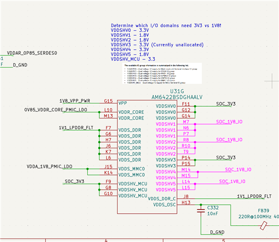
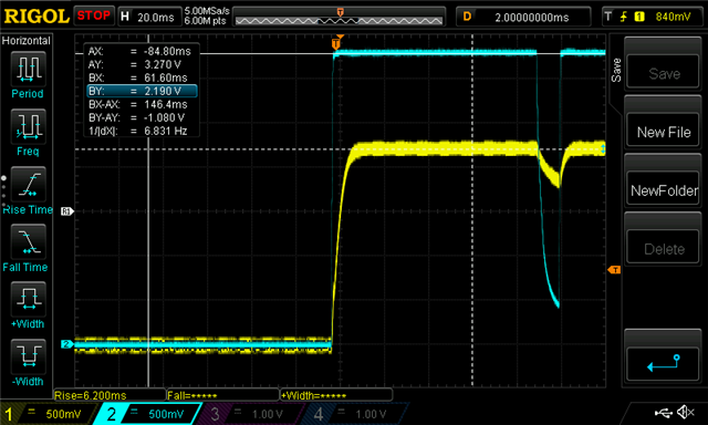
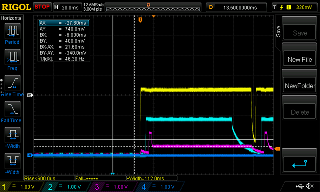
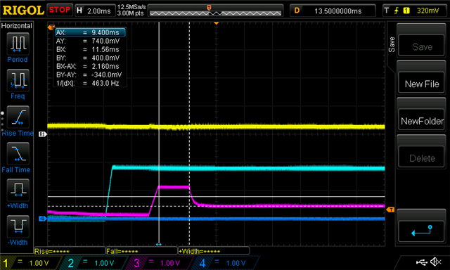
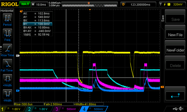
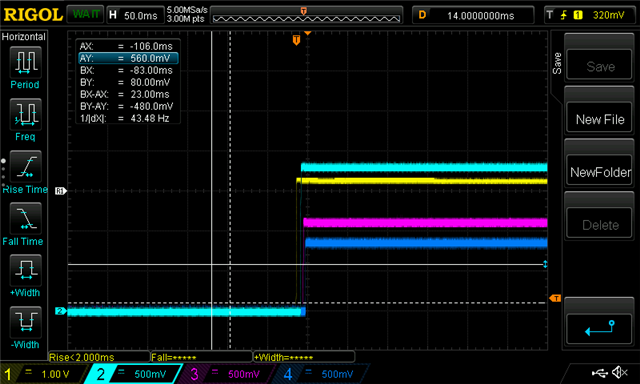
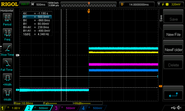
Hi all - I have a schematic review request for a design with a AM64X processor. Right now we're seeing the TPS6522053 unable to fully ramp up, and we're hoping that we can get some insights as to what might possibly be going on.

Thanks,

James

  • Hello James, 

    Thank you for the query.

    Did you share the PDF searchable schematics?

    Regards,

    Sreenivasa

  • Hi Sreenivasa, I've sent the searchable schematics in PDF form via a private message to you now. Thanks!

  • Hi Sreenivasa - it looks like I'm getting an unexpected voltage coming from the AM6442, out of the IO supply (the thread is over here  TPS65220: TPS6522053RHBR Failed to generate power supply rails )

    Doing a cursory check, it does look like I have a failure where I tied a an IO supply to the incorrect supply rail - I expected VDDSHV4 to be tied to 3V3, but it is instead supplied from the 1V8 rail.
    That said - we aren't at the point where the PMIC supplies 3V3 to the AM6442 yet - so yep, a bit weird.

  • Hello James, 

    The PMIC may not be starting in case the residual voltage is present.

    Can you probe the PMIC outputs to see if the PMIC tries to restart and then shutdown.

    The pullup voltage referenced to any of the IO is expected to match the IO supply for IO group (VDDSHVx)

    Regards,

    Sreenivasa

  • So the PMIC does start - it tries three times (we go through it in the other thread with oscope shots and everything :D) and then stops.
    Doing some more probing at various points just now - the PMIC does (briefly) turn on the enable for the 3V3 switch, providing the AM64 (along with all of other consumers and pullups) with 3V3 power in those pulses. 
    My best guess would be that the pullups on the IOs associated with VDDSHV4 (tied to 3V3) are pulling up the SOC_1V8_IO rail. This should be testable if I remove pullups for I/Os associated VDDSHV4 (or perhaps just cut the traces for the I/Os, since with the wrong sourced voltage it isn't really going to be any help) - I would then expect the voltage to no longer be present on the SOC_1V8_IO rail. Does that seem reasonable?

  • Hello James, 

    The rails before the residual voltage is observed is expected to come up.

    residual voltage is likely to occur when the IO supply group is referenced to 1.8V and the IO pullup has 3.3V or if any of the IO inputs are available much before the SOC supplies ramp.

    Regards,

    Sreenivasa

  • Hello James, 

    Which IOs are you seeing that is connected to 3.3V  for VDDSHV4?

    Regards,

    Sreenivasa

  • Hi Sreenivasa, the following IOs are involved with VDDSHV4. I've gone through and taken some actions, and actually about to turn on and see whether or not I would get voltage on SOC_1V8_IO here in the next few minutes. I suspect/expect that N20, N21, M20, P20, N18 are possibly the issues.

    PIN SigName Pullup Resistor Pulldown resistor How to address Cut completed Lead attached Component Removed
    N20 RTC_interrupt R381 - this resistor has to be removed; possibly interrupt needs to be cut (likely not, as it looks to pull the line down) - Yes
    N21 ROUTE_DIRECT R258 - cut IO and attach lead/item to resistor in order to externally control at later point for test - this I/O can be cut near processor on the back side Yes -
    N19 RESET_PWR_SOLENOID - R22 do not cut – should be able to control this - - -
    M19 RESET_PWR_CELL - R226 do not cut – should be able to control this - - -
    M18 not connected - - - - - -
    M20 HUB_RESET R263 - cut IO, keep this up (down resets device) (possibly attach lead to externally control), cut it on the back side near C355 Yes - -
    P21 SIM_SEL - - (no pullup!) - dont work with it right now - - -
    P20 RESET_PHY_0 R455 - disconnect I/O , possibly attach lead to externally control later for test Yes - -
    N18 RESET_PHY_1 R270 - disconnect I/O , possibly attach lead to externally control later for test Yes - -
    K17 CELL_PWRKEY - R210 pulled down - disconnect I/O , attach lead to externally control later for test Q21 pin 1 - unable to cut, as this is under Q21, leave it alone (min turn on is 1.1V, so this could be turned on using 1V8) - - -
    L17 CELL_RESETKEY - R421 pulled down - disconnect I/O , attach lead to externally control later for test Q22 pin 1 - this may be possible to cut, but leave alone (min turn on is 1.1V, so this could be turned on using 1V8) - - -


  • So, the voltage on SOC_1V8_IO is still present (keeping in mind that FB40 is removed from the board, the voltage isn't coming in from the PMIC 1V8). Here are some shots of the INT_3V3_SYS (from pin 8 of U59) vs SOC_1V8_IO (from pad2 of FB40). SOC_1V8_IO is about 2.2V still.


    I suppose the next step would be to review all of the other IOs sourced from 1V8 banks and make sure that none of them are mistakenly pulled up to 3V3.

  • Hello James,

    The 1.8V you are seeing is due to voltage feed.

    I suppose the next step would be to review all of the other IOs sourced from 1V8 banks and make sure that none of them are mistakenly pulled up to 3V3.

    Correct.

    Regards,

    Sreenivasa