


Hi, every one, I have a question about DDR3 trace routing with the DM816x EVM Schematic.
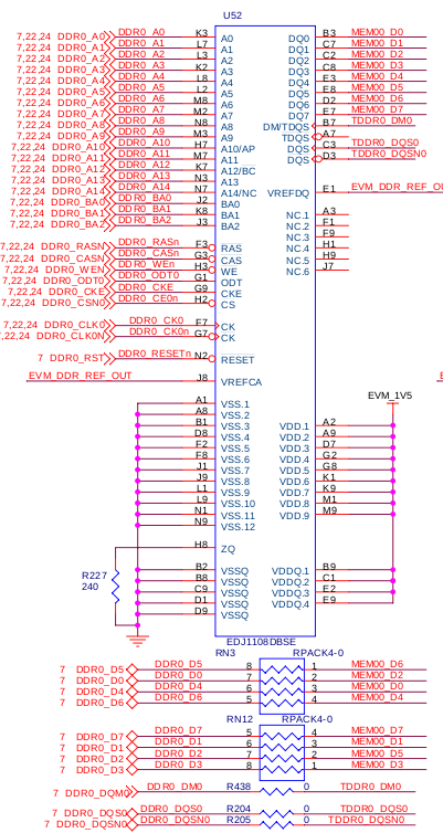
As usual, we may roue the DQ lines as:
cpu side ram side
DDR0_D0 -> MEM00_D0
DDR0_D1 -> MEM00_D1
DDR0_D2 -> MEM00_D2
DDR0_D3 -> MEM00_D3
DDR0_D4 -> MEM00_D4
DDR0_D5 -> MEM00_D5
DDR0_D6 -> MEM00_D6
DDR0_D7 -> MEM00_D7
but in the EVM Schematic, the DQ signal line is routing as the picture show below
cpu side ram side
DDR0_D0 -> MEM00_D2
DDR0_D1 -> MEM00_D1
DDR0_D2 -> MEM00_D5
DDR0_D3 -> MEM00_D3
DDR0_D4 -> MEM00_D0
DDR0_D5 -> MEM00_D6
DDR0_D6 -> MEM00_D4
DDR0_D7 -> MEM00_D7
why this happen?
qing
2012-1-30
