This thread has been locked.
If you have a related question, please click the "Ask a related question" button in the top right corner. The newly created question will be automatically linked to this question.
Hi
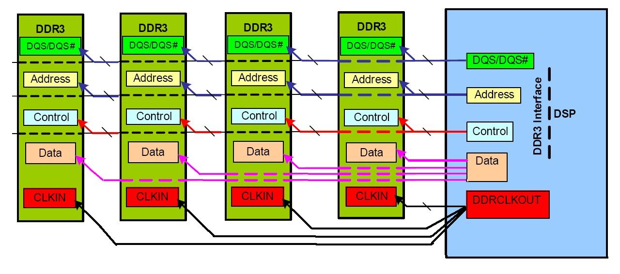
We are in the process of designing a board with 6678 DSP along with DDR3 interface
1. Please suggest how to route clock line to the ddr3 chips ..either follow method1 or method2 as attached
2. Also please suggest in the length matching group , clock and address line should be of same length (OR)
clock line length should be greater than address line length by 2 inches....
Method1
Method 2
Thanks
Mahendra,
Neither figure is totally correct. Data group nets will be point to point. Address, Command, Control and Clock group nets will all be routed in a fly-by confirguration with VTT termination. The 2 inch limitation is not valid.
More information is available in the following forum thread and the referenced documents and spreadsheets: http://e2e.ti.com/support/dsp/c6000_multi-core_dsps/f/639/t/245304.aspx.
Tom