This thread has been locked.

If you have a related question, please click the "Ask a related question" button in the top right corner. The newly created question will be automatically linked to this question.

AM620-Q1: OSPI NAND Flash Selection Guide & Reset Pin

Part Number: AM620-Q1

Hello team,

is there some type of selection guide or a table showing compatible flash devices to AM620-Q1 using OSPI?

Specifcally in the TRM the following requirement is mentioned: "When using a OSPI\xSPI\QSPI\SPI flash device greater than 128Mb which supports 3-byte and 4-byte addressing modes, a flash device package with a RESET signal (NOR type memories only) must be used "

In the following E2E there are some NAND Flash recommendations: AM62A7-Q1: Automotive NAND Flash Selection with Available Driver - Processors forum - Processors - TI E2E support forums 

The recommended NAND flashes do not have a reset pin so I wonder how the TRM requirement can be fulfilled with these NAND flashes. Or does the TRM mean that there is only a RESET signal needed when NOR flashes are used.

Which NAND flashes do you recommend? I saw on the Starterkit this NAND flash is used: W35N01JW_Datasheet_Brief.pdf . For the application the memory is not enough so another memory is needed.

 

  • Hi Schoengarth,

    Thank you for the query.

    To my knowledge, the TI can  provide recommendations for Flash OSPI\xSPI\QSPI\SPI  NOR- and NAND- memory devices that have been tested on TI manufactured starter kits and EVMs.

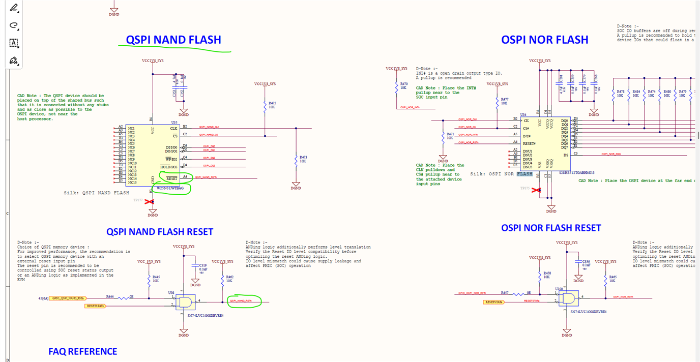
    One example for tested QSPI NAND Flash is the AM62LEVM evaluation board, where QSPI W25N01JWTBAG is used. It has a RESET pin. 

    The main reason to recommend Flashes with Reset pin is NOT the type of the logic -NOR, but the restriction of AM620-Q1 ROM code to operate only in 3-Byte addressing mode when booting from OSPI/QSPI/xSPI/SPI Flashes and the need the Flash memory to switch back from 4-Byte (non-ROM boot stages) to 3-Byte addressing mode when software and warm reset occurs.

    I will follow-back later today with more information.

    I hope this helps.

    Best Regards,

    Anastas Yordanov

  • Hello Anastas,

    Thank you. Do you have more information on the rest of my questions now?

    Best regards,

    Til

    Which NAND flashes do you recommend

    In the following E2E there are some NAND Flash recommendations: AM62A7-Q1: Automotive NAND Flash Selection with Available Driver - Processors forum - Processors - TI E2E support forums 

    The recommended NAND flashes do not have a reset pin so I wonder how the TRM requirement can be fulfilled with these NAND flashes.

  • Additionally: 

    If I understand the Technical Reference Manual correct, reset pin is only need for OSPI\xSPI\QSPI\SPI Boot option. The mentioned 8Gbit NAND MT29F8G08ADAFAH4 is GPMC NAND Boot option, where a reset pin is not needed.


    I have a question regarding OSPI\xSPI\QSPI\SPI Boot option:


    • Could you please check, if there is a work around if reset pin is not available on NAND flash? E.g reset of NAND by switching of VCC?


    I have two questions regarding GPMC NAND Boot:


    • Reset pin is not needed for GPMC NAND option?
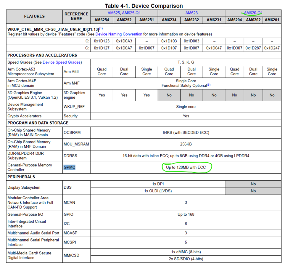
    • In the datasheet is mentioned, that GPMC supports ECC only up to 128MB. Does this mean for the MT29F8G08ADAFAH4 ECC is not available?
  • Hi,

    For OSPI part number selection guides, please refer to the below E2E threads and any other you can find on E2E. TI is not maintaining a list of supported or tested memories.

     https://e2e.ti.com/support/processors-group/processors/f/processors-forum/1524081/am62l-customer-am62l-board-how-to-choice-qspi-nand-flash/5868399

     [FAQ] TDA4VM: Is there a guide to choosing the right OSPI Flash parts that are supported on Jacinto 7? 

    Could you please check, if there is a work around if reset pin is not available on NAND flash? E.g reset of NAND by switching of VCC?

    Looks like TRM was recently updated with (NOR memories only) and this is not strictly required by ROM, however I think RESET pin is still recommended as per screenshot from Anastas. Yes, Power cycling is also an option.

    Reset pin is not needed for GPMC NAND option?

    I think usually parallel memories are not offered with Reset pins because of the much simpler internal logic. Most of the logic is in the GPMC controller inside the SoC.

    In the datasheet is mentioned, that GPMC supports ECC only up to 128MB. Does this mean for the MT29F8G08ADAFAH4 ECC is not available?

    The datasheet mentions limitation of total memory size limited by address pins pinned out on this device and not a limitation to ECC. This however should be related to GPMC NOR and not GPMC NAND as NAND protocol is different and all pins required by NAND are pinned out.

    ROM code supports parallel NANDs under following conditions:

    Regards,

    Stan

  • Hello Stan,

    thank you!

    I have some follow up questions based on your response:

    1. Can you please confirm that for NAND Flash 2 Gbyte is the maximum supported size and for NOR flash 128MB is the maximum supported size with GPMC?

    2. Do we have experience / Do you see that other customers use NAND flash and NOR flash in parallel? NOR for ROM and NAND for the application

    2a If yes, do we have some proof of concept or maybe some EVM where this is done?

    3. Does it make sense to only have NAND over GPMC for both ROM and Application?

    4. If only NAND flash is used, how do you see the security/safety aspect? As NAND flash can be more easily compromised than NOR.

    5. In the TRM it is specified that GPMC is setup to comply with mode 0 timing for NAND flash. Does that mean there is some limitation in operation frequency or can the 133MHz always be achieved with GPMC?

  • Some additional details:

    1.  Can you please confirm that for NAND Flash 2 Gbyte is the maximum supported size and for NOR flash 128MB is the maximum supported size with GPMC?

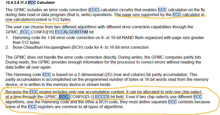
    1a And if 2Gybte NAND Flash are supported, can you please confirm that hardware ECC is supported across the full 2Gbyte

    2. Do we have experience / Do you see that other customers use NAND flash and NOR flash in parallel? NOR for ROM and NAND for the application

    2a If yes, do we have some proof of concept or maybe some EVM where this is done?

    2b) Does the SoC's Boot ROM support a boot sequence that can be configured to prioritize a specific Chip Select line (e.g., CS0), allowing us to reliably initiate the boot process from the NOR flash?

    2c) Can the GPMC be configured to manage two distinct device profiles concurrently on separate chip-select regions? For example, an asynchronous 16-bit NOR on CS0 and a synchronous 8-bit NAND with active ECC on CS1.

    3. Does it make sense to only have NAND over GPMC for both ROM and Application?

    4. If only NAND flash is used, how do you see the security/safety aspect? As NAND flash can be more easily compromised than NOR.

    5. In the TRM it is specified that GPMC is setup to comply with mode 0 timing for NAND flash. Does that mean there is some limitation in operation frequency or can the 133MHz always be achieved with GPMC?

    Timing Mode 0 implies a maximum transfer rate of 10 MT/s.

    • 5a) Can you confirm that the initial boot process, managed by the SoC's internal Boot ROM, is restricted to asynchronous ONFI Timing Mode 0?
    • 5b) After loading an initial bootloader, is it possible to reconfigure the GPMC at runtime to address the NAND flash using a higher-performance timing mode?
    • 5c) Maximum Supported Mode: For application-level operation, what is the maximum supported ONFI mode?
  • Hi Til,

    Sorry, I will not be able to answer all the questions today EOB. I will come back to you early next week.

    Regards,

    Stan

  • Hello Stan,

    thanks and no problem.

    An answer today (at least a partial answer) would be highly appreciated as this is an urgent topic at the customer.

    Best regards,

    Til

  • Hello Til,

    Thanks for your questions.

    1.  Can you please confirm that for NAND Flash 2 Gbyte is the maximum supported size and for NOR flash 128MB is the maximum supported size with GPMC?

    1a And if 2Gybte NAND Flash are supported, can you please confirm that hardware ECC is supported across the full 2Gbyte

    You may want to refer to the below GPMC FAQ thread: Maximal size of AM62x GPMC supported NOR,NAND and pSRAM memories.

    The AM62x (AD[31:16] are not output on SoC pins) and the 32-bit multiplexed data/address Flash memories are not supported by the AM62x GPMC. Therefore according to the FAQ table the maximal supported size is the size for 16-bit NOR Flash memories with multiplexed address and data - 128 MBytes. For a total of 4 CS this means a total of 512 MBytes NOR-addressable area by the GPMC. According to the table in the thread, the  maximal supported size for the 16-bit and 8-bit NANDs is NOT limited for the application software. It is only limited to 2 GBytes for the AM62x ROM booting.

    2. Do we have experience / Do you see that other customers use NAND flash and NOR flash in parallel? NOR for ROM and NAND for the application

    2a If yes, do we have some proof of concept or maybe some EVM where this is done?

    To my knowledge, connection of a NAND and NOR memories to different CS of the GPMC is rather rarely used with the AM62x or other newer SITARA processors on TI EVMs and custom boards. 

    - I need to check if there is additional reason - like  SI or other hardware limitations for the AM62x GPMC to have attached NAND/NOR or FPGA to more than one of its chip selects.

    There are other interfaces which are faster in booting than GPMC - like OSPI or eMMC, or which are used as alternative to a GPMC memory storage. Nevertheless, the following FAQ example with AM62 L3 EVM demonstrates a concept in which AM62x ROM boots code from an 8-bit ONFI 1.0 NAND (2-GBytes or less) and switches CS to continue to operate with a NAND daughter board.

    GPMC Booting U-Boot from 8-bit ONFI NAND + NAND daughter card 

    I could not find an example in which a NOR flash used for ROM booting over GPMC is combined with a NAND used for data storage over GPMC.

    Examples of mixing NON-GPMC and GPMC interface NAND and NOR memories: 

    - NOR Flash will be attached to an OSPI interface, and a parallel NAND flash memory connected to GPMC, used for application purposes.

    - An 8-bit ONFI 1.0 compliant NAND flash memory used for ROM booting code over GPMC combined with an eMMC memory used for data storage operations.

    2b) Does the SoC's Boot ROM support a boot sequence that can be configured to prioritize a specific Chip Select line (e.g., CS0), allowing us to reliably initiate the boot process from the NOR flash?

    I am not sure if I correctly understand ? Are you asking about a GPMC multiple chip-select configuration in which different CS are used during different stages ?  According to the AM62x TRM / Chapter, Initialization, the AM62x ROM can boot code from a 16-bit non-mux NOR flash memory detected ONLY on the GPMC0_CSn0 (the only allowed NOR-type for the ROM to boot from). 

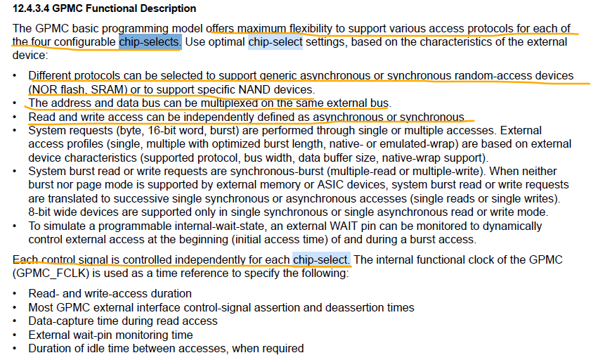
    2c) Can the GPMC be configured to manage two distinct device profiles concurrently on separate chip-select regions? For example, an asynchronous 16-bit NOR on CS0 and a synchronous 8-bit NAND with active ECC on CS1.

    The following  AM62x TRM Section, GPMC Functional Description specifies:

    While this might be physically possible according to the above stated level of independence between the 4 different GPMC chip select channels, I am not completely sure if there aren't software limitations to do this. This question may need to be referred for clarification  to the GPMC software team.

    Does it make sense to only have NAND over GPMC for both ROM and Application?

    For applications and ROM this might not be as efficient  as having both NOR and NAND memories attached on two different chip selects of the GPMC. The main advantage because of the NOR flash read speeds during boot. Anyway the AM62x ROM does NOT support GPMC XIP booting and ECC for NOR flash. In terms of  both MCU-PLUS, LINUX SDK or AUTOSAR MCAL I need to check if there are SPL drivers which support NOR booting over GPMC. Please specify which SDK / framework do you need information about ?   

    4. If only NAND flash is used, how do you see the security/safety aspect? As NAND flash can be more easily compromised than NOR.

    The safety drawbacks can be partially compensated by the ECC calculations performed by the ELM. I still need to internally discuss / research more regarding security advantages / disadvantages of the GPMC interface. 

    5. In the TRM it is specified that GPMC is setup to comply with mode 0 timing for NAND flash. Does that mean there is some limitation in operation frequency or can the 133MHz always be achieved with GPMC?

    Can you please refer me to the appropriate section in the AM62x TRM ? Is this the case when: GPMCFCLKDIVIDER = 0 ?

    Thanks

    Best Regards

    Anastas Yordanov

  • Hello Anastas,

    thanks a lot of the detailed response. I think that probably NOR over OSPI for boot and NAND over GPMC makes the most sense then.

    I will follow up when I have further feedback from the customer.

    Regarding 4): 

  • Hello Til,

    Thank you for the note and looking forward to your inputs.

    Regards,

    Sreenivasa

  • Kallikuppa,

    can you please respond to 4)

    I.E. is only mode 0 timing possible with NAND over GPMC or can this be changed?

  • Hi Til,

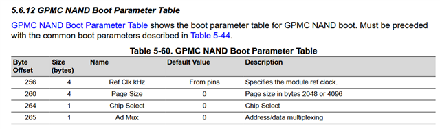
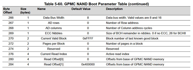
    ROM code uses several RAM locations to store parameters for each boot mode that can be changed by user and taken into account after subsequent warm booting.  Unfortunately  can't find anything about timing in the GPMC NAND boot parameter table:

    Regards,

    Stan

  • Hello Stan,

    with mode 0 timing the frequency would be restricted to 10Mhz - but it is true that the full 133MHz of GPMC can be used, correct?

  • Hi Til,

    I'm still not sure what's mode 0 for GPMC. I need to check internally. I remember earlier Sitaras booted at 66 MHz and this can be adjusted later in SW/SBL.

  • Taking this offline.

    BR,

    Til