This thread has been locked.

If you have a related question, please click the "Ask a related question" button in the top right corner. The newly created question will be automatically linked to this question.

DDR3 Setting with Boot Table via I2C master boot

Hi

Are there any infomation about DDR Configuration Table Setting for ROM Bootloader?

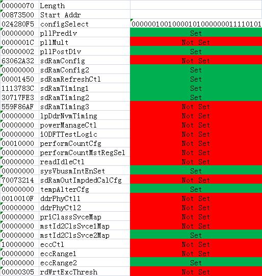
ex.  I can't understand about "config 2" field  . DDR Controller has only one SDRAM Configuration Register (SDCFG).

----

I'm trying to configure DDR3  on ROM Bootloader while booting I2C Master Mode.

I build myProg.out and convert to myProg2.b (Ascii Hex file)  , using hex6x.exe.

and, I manualy edit it ,and insert a DDR Confiiguration section between Entrypoint and first section of My Program.

This section's first DWORD named "Enable Bitmap"  is set to "0x0000 0003" to set both PLL and SDRAM.

next, I continue convert MyProg.bin to MyProg.bin using lbl Utils (bconvert64, b2i2c, ,,romparse.etc..)

After tihs, Our board dosen't boot. and JTAG Connection is refused.

Simple myProg.bin (without DDR Configuration section) can bootup.

thank you

  • I sloved by myself.

    first of all. DDR Configuration shown in "BootLoader Users Guide"( SPRUGY5A  p.2-4)  is wrong. I 've read SRC of Shannon boot loader. and I found first PLL setting must have 3 DWORDs.

    Next, post div of ddr PLL Setting  must be "2" although "0" operates.
    It is because it is used for calculation of waiting time.

    here is my DDR Configuration in boot table.
    00 00 00 70 00 87 35 00 02 42 80 F5 00 00 00 00 00 00 00 20 00 00 00 02
    63 46 2A 32 00 00 00 00 00 00 14 50 11 13 78 3C 30 4F 7F E3 55 9F 84 9F
    00 00 00 00 00 00 00 00 00 00 00 00 00 01 00 00 00 00 00 00 00 00 00 00
    00 00 00 00 70 07 32 14 00 00 00 00 00 10 01 0F 00 00 00 00 00 00 00 00
    00 00 00 00 00 00 00 00 10 00 00 00 00 00 00 00 00 00 00 00 00 00 03 05

    Will you please point out any mistakes to me?
    Pls take notice that the Target board is not EVM,DSK but our original board.

    kazunori

  • I'm stuck with a similar problem; I'm trying to get the EVM to boot from Ethernet in ROM boot mode (without the EEPROM Intermediate Boot Loader) using hex6x, bconvert64x, bootpacket and finally pcsendpkt (these tools are in the MCSDK). Kazunori, you've probably saved me a week of bashing my head against the wall, thank you!

    Can a TI employee acknowledge this (very serious) documentation error, and kindly offer a correct DDR configuration for the EVM6678? It is not at all obvious how to convert the existing GEL or platform-lib C code into the format shown in the post above. Despite my efforts to do this, my program which loads fine in JTAG starts running but soon crashes when booting over Ethernet, probably due to some incorrect DDR or PLL setting.

    Also, is there a better method to insert this configuration into the binary than hand editing the results of hex6x?

    Thanks,

    -itay

  • Since it is very difficult to understand from the GEL code (or the bootloader source code) what values are supposed to be loaded into the DDR and PLL registers my approach has been to either read the values present in the registers after the GEL has done its initializations (through JTAG), or trial and error, or a combination of both.

    I now have the following configuration. It seems to work but I am not certain of its correctness. (Least certain are the PLL values, which are the last three DWORDs in the first line.) I will appreciate any correction and hope that it will be of use to others in the community.

    00 00 00 70 00 87 35 00 02 42 80 F5 00 00 00 00 00 00 00 1C 00 00 00 02
    63 06 2A 32 00 00 00 00 00 00 14 50 11 13 78 3C 30 71 7F E3 55 9F 86 AF
    00 00 00 00 00 00 00 00 00 00 00 00 00 01 00 00 00 00 00 00 00 00 00 00
    00 00 00 00 70 07 32 14 00 00 00 00 00 10 01 0F 00 00 00 00 00 00 00 00
    00 00 00 00 00 00 00 00 10 00 00 00 00 00 00 00 00 00 00 00 00 00 03 05

    To understand the format of this table, see document sprugy5 (boot loader) section 2.5.3. The above table is a single COFF section in that context. The destination address is explained in Table 2-2 (CorePac0 Memory Usage by the ROM Bootloader) and the contents are detailed (incorrectly, see Kazunori's corrections above and struct bootEmif4Tbl_s in the file tiboot.h of the bootloader source code) in Table 2-3 (DDR Configuration).

    This table needs to be inserted into the file created as a result of running hex6x on your .out file, immediately after the first 4 bytes (which are the run address).

    -itay

  • hi itay.
    Our board works in Big endian mode.

    EVM works in little endian. I'm not sure that the hex file must be converted to little endian.

    Have you checked?

    Kazunori.

  • Oh,you wrote that  the configuration seems to work.
    My indication was irrelevant.
    sorry.

  • Hi,Italy,

    I've tried your DDR configuration table,and that really works well on evm6678 but not on evm6670. Is there any difference between Shannon and Nyquist boards in configuration table ?

    thanks.

  • Hello striker Qian,

    Look at the second dword in the first line of the table. You will see 00 87 35 00. This is the big endian representation of the address 0x873500 which is where this table will be loaded in memory during boot. On the C6678 this is where the ROM boot loader expects the DDR configuration table, but this address is incorrect for the C6670. The address is calculated according to sprugy5b, Table 2-2:

    RBL_DDRCONFIG_ADDR = L2SRAM_TOP - RBL_DATASIZE + RBL_DDRCONFIG_OFFSET

    On all Keystone devices RBL_DATASIZE is 0xD240 (this is given just above Table 2-2. Note that the value written there is 0xD23F which is actually off by 1 byte).

    The RBL_DDRCONFIG_OFFSET is 0x740 as shown in that table.

    L2SRAM_TOP is 0x880000 on the C6678 but 0x900000 on the C6670. So we get:

    RBL_DDRCONFIG_ADDR = 0x900000 - 0xD240 + 0x740 = 0x8F3500

    So simply change the 00 87 35 00 to 00 8F 35 00.

    With that change, the DDR configuration table will become effective, though I can't promise that the register values are 100% correct as I have no experience with the 6670 device.

    Good luck,

    -itay

  • Hi,Itay:

    Thank you for your kind help and I finally boot the evm6670 board with ddr initialized. However there's still a few things I want to know. :) What does the first line"00 00 00 70"mean in this table? I can't find any information in any docs or "tiboot.h"and that's why I can't make sense of dword two 0x00873500. Where did you get the information of these two dwords?

    many thanks again!

  • The tiboot.h file is part of the ROM Boot Loader source code package, which may be found at http://processors.wiki.ti.com/index.php/Keystone_Device_Architecture .

    When the boot loader loads an image to the device it expects data in the form of blocks, with each block having a header indicating the size and destination address of that block. So, in this case 0x00000070 is the size and 0x00873500 is the destination address. See sprugy5b section 2.5.

    -itay

  • Hi Itay,

    I compared your seeting with the structure defined in "tiboot.h", and got the following table.

    Is that anything that I misunderstood?

    Alif

  • Alif,

    Your translation from the bitmap of configSelect to the Set and Not Set (green and red) indicators is incorrect. Bit 0 of configSelect controls the three PLL settings. Bit 1 has no effect. From bit 2 and on it behaves as expected, with each bit controlling one register starting from sdRamConfig. See the definitions BOOT_EMIF4_ENABLE_pllCtl, BOOT_EMIF4_ENABLE_sdRamConfig etc. in the tiboot.h file.

    So the indicators in the right column need to be shifted down one slot, and all three PLL settings should be changed to green (Set).

    -itay

  • Itay,

    Thank you very much.

    Nowadays, I am trying to boot my 6614 EVM via ethernet. I can not find a right way to initialize DDR3 before loading my application.

    From the datasheet of 6614 and 6670, it seems rather similar. And they all belong to C66 family, the RBL should have the same strategy.

    I tried the setting in your post, but it can not work.

    I am puzzled.

    Alif

  • Have you tried changing the Start Address value from 00873500 to 008F3500 like I explained earlier? It looks like you need to do that on the 6614 because it has 1MB L2 memory.

  • Dear all,

    In that first line:

    "00 00 00 70 00 87 35 00 02 42 80 F5 00 00 00 00 00 00 00 1C 00 00 00 02"

    Why is "1C" the value for DDR3_PLLM?. This means x28 (27+1), which equals an output frequency of 66.67 * 28 / 2 = 933MHz, so this is DDR3 working at 1866MHz data rate. I think that DDR3 chips in EVM are 1333 rate, so I would think that the correct value would be 0x13 (19+1=20, 66.67*20/2 = 1333MHz)

    Regards,

    Ricardo