
- Ask a related questionWhat is a related question?A related question is a question created from another question. When the related question is created, it will be automatically linked to the original question.
This thread has been locked.
If you have a related question, please click the "Ask a related question" button in the top right corner. The newly created question will be automatically linked to this question.
For the Keystone I Devices, there are some leveling issue described in Silicon Errata below.
TMS320C6678 Multcore Fixed & Floating-Point DSP Silicon Errata (Revs 1.0, 2.0) (Rev. F)
http://www.ti.com/lit/er/sprz334f/sprz334f.pdf
Advisory 9 DDR3 Automatic Leveling Issue
Advisory 26 DDR3 Incremental Write Leveling Issue
Advisory 9 describes the Read Data Eye Training issue. There are the three leveling types in the Automatic Leveling, i.e. Write Leveling, Read DQS Gate Training and Read Data Eye Training. This issue is only related to the Read Data Eye Training.
For Workaround 1 in Advisory 9, the Partial Automatic Leveling is used.
For Workaround 3 in Advisory 9, the Partial Automatic Leveling with the Incremental Leveling is used.
These details are described in Application Note below.
In addition, the Application Note describes using the Full Automatic Leveling with the Incremental Leveling for the latest KeyStone devices.
The devices supporting these leveling mode are described in the Table 3.
KeyStone DDR3 Initialization (Rev. A)
http://www.ti.com/lit/an/sprabl2a/sprabl2a.pdf
Table 3 Leveling Modes Supported
3.2 Partial Automatic Leveling
3.2.1 Executing Partial Automatic Leveling
3.2.2 Enabling Incremental Leveling with Partial Automatic Leveling
3.3 Full Automatic Leveling
For the more optimum leveling, which of these leveling modes should be used? Should the Full Automatic Leveling with the Incremental Leveling be used?
The timeout register bits in the DDR3 Memory Controller Status Register can be read to verify that the leveling completed as expected.
DDR3 Memory Controller for KeyStone Devices User's Guide (Rev. C)
http://www.ti.com/lit/ug/sprugv8c/sprugv8c.pdf
4.2 DDR3 Memory Controller Status Register (STATUS)
Can the reading these bits ensure the detection of the failure of the leveling? Should the data written be verified? If so, how should it be verified? Should all addresses be verified?
For the DDR3 Register values and the DDR3 PHY initial values, two spreadsheets below are used.
DDR3-Register-Calc-v4
http://e2e.ti.com/cfs-file.ashx/__key/communityserver-discussions-components-files/639/6013.DDR3-Register-Calc-v4.xlsx
DDR3-PHY-Calc-v10
http://e2e.ti.com/cfs-file.ashx/__key/communityserver-discussions-components-files/639/8130.DDR3-PHY-Calc-v10.xlsx
Are these spreadsheets the latest version?
Best regards,
Daisuke
Hi,
I'm sorry, I made a mistake for the Workaround 3 in Advisory 9.
For Workaround 3 in Advisory 9, the Full Automatic Leveling with the Incremental Leveling is used for the latest KeyStone devices. The details are described in Application Note below.
KeyStone DDR3 Initialization (Rev. A)
http://www.ti.com/lit/an/sprabl2a/sprabl2a.pdf
3.3 Full Automatic Leveling
In this leveling mode, Incremental leveling is used for the Read DQS Gate Training and the Read Data Eye Training and can work in substitution for Full Automatic Leveling that has the Read Data Eye Training issue. For the more optimum leveling, this leveling mode should be used.
Note: Incremental leveling cannot be used for the Write Leveling because there is the Incremental Write Leveling Issue described in the Silicon Errata Advisory 26.
Is my above-mentioned understanding correct?
Please give me an answer for my questions as soon as possible.
Daisuke Maeda said:The timeout register bits in the DDR3 Memory Controller Status Register can be read to verify that the leveling completed as expected.
DDR3 Memory Controller for KeyStone Devices User's Guide (Rev. C)
http://www.ti.com/lit/ug/sprugv8c/sprugv8c.pdf
4.2 DDR3 Memory Controller Status Register (STATUS)Can the reading these bits ensure the detection of the failure of the leveling? Should the data written be verified? If so, how should it be verified? Should all addresses be verified?
Daisuke Maeda said:For the DDR3 Register values and the DDR3 PHY initial values, two spreadsheets below are used.
DDR3-Register-Calc-v4
http://e2e.ti.com/cfs-file.ashx/__key/communityserver-discussions-components-files/639/6013.DDR3-Register-Calc-v4.xlsxDDR3-PHY-Calc-v10
http://e2e.ti.com/cfs-file.ashx/__key/communityserver-discussions-components-files/639/8130.DDR3-PHY-Calc-v10.xlsxAre these spreadsheets the latest version?
Your prompt reply would be appreciated.
Best regards,
Daisuke

Hi,
I have some more questions.
For Workaround 3 in Advisory 9, Incremental leveling is used only for the Read Data Eye Training.
In the Application Note, Incremental leveling is used for both the Read DQS Gate Training and the Read Data Eye Training.
For the more optimum leveling, should both the Read DQS Gate Training and the Read Data Eye Training be performed?
For Workaround 3 in Advisory 9, if desired, the initialization routine can disable the Incremental leveling after it works.
In the Application Note, it is highly recommended for long-term DDR3 operation stability at the higher operating rates that the Incremental leveling occurs periodically during normal operation.
KeyStone DDR3 Initialization (Rev. A)
http://www.ti.com/lit/an/sprabl2a/sprabl2a.pdf
3 Leveling Execution
For the more optimum leveling, should the Incremental leveling occur periodically during normal operation?
Best regards,
Daisuke
Hi,
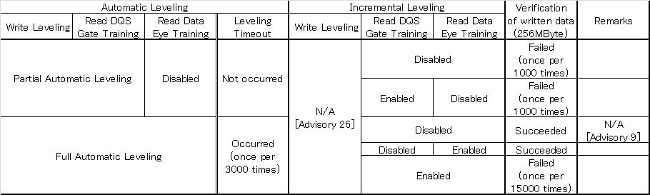
Some custom boards have the DDR3 issue. After initialization, the written data are verified. The following table shows those worst cases.

For the more optimum leveling, after the Full Automatic Leveling, the Incremental Leveling with the Read DQS Gate Training and the Read Data Eye Training should be used. But this leveling mode may fail. Which of the leveling modes should be used?
Please see DDR3Init() in the attached source file for the initialization sequence. Does it have any mistake?
/******************************************************************************
* Copyright (c) 2010-2011 Texas Instruments Incorporated - http://www.ti.com
*
* Redistribution and use in source and binary forms, with or without
* modification, are permitted provided that the following conditions
* are met:
*
* Redistributions of source code must retain the above copyright
* notice, this list of conditions and the following disclaimer.
*
* Redistributions in binary form must reproduce the above copyright
* notice, this list of conditions and the following disclaimer in the
* documentation and/or other materials provided with the
* distribution.
*
* Neither the name of Texas Instruments Incorporated nor the names of
* its contributors may be used to endorse or promote products derived
* from this software without specific prior written permission.
*
* THIS SOFTWARE IS PROVIDED BY THE COPYRIGHT HOLDERS AND CONTRIBUTORS
* "AS IS" AND ANY EXPRESS OR IMPLIED WARRANTIES, INCLUDING, BUT NOT
* LIMITED TO, THE IMPLIED WARRANTIES OF MERCHANTABILITY AND FITNESS FOR
* A PARTICULAR PURPOSE ARE DISCLAIMED. IN NO EVENT SHALL THE COPYRIGHT
* OWNER OR CONTRIBUTORS BE LIABLE FOR ANY DIRECT, INDIRECT, INCIDENTAL,
* SPECIAL, EXEMPLARY, OR CONSEQUENTIAL DAMAGES (INCLUDING, BUT NOT
* LIMITED TO, PROCUREMENT OF SUBSTITUTE GOODS OR SERVICES; LOSS OF USE,
* DATA, OR PROFITS; OR BUSINESS INTERRUPTION) HOWEVER CAUSED AND ON ANY
* THEORY OF LIABILITY, WHETHER IN CONTRACT, STRICT LIABILITY, OR TORT
* (INCLUDING NEGLIGENCE OR OTHERWISE) ARISING IN ANY WAY OUT OF THE USE
* OF THIS SOFTWARE, EVEN IF ADVISED OF THE POSSIBILITY OF SUCH DAMAGE.
*
*****************************************************************************/
/******************************************************************************
*
* File Name: Setup_Pllc.c
*
* Description: This contains TMS320C6678 specific functions.
*
******************************************************************************/
/************************
* Include Files
************************/
#include "main.h"
#include "Setup_Pllc.h"
uint32_t dsp_frequency;
static Bool MemoryCheck1();
static Bool MemoryCheck2();
extern unsigned int RetryCount0;
extern unsigned int RetryCount1;
extern unsigned int RetryCount2;
extern unsigned int RetryAddress[];
extern unsigned long long RetryValue[];
extern unsigned long long RetryNextValue[];
extern unsigned int RetryIndex;
void delay(uint32_t usecs)
{
int32_t delayCount = (int32_t) usecs * dsp_frequency;
int32_t start_val = (int32_t) CSL_chipReadTSCL();
while (((int32_t)CSL_chipReadTSCL() - start_val) < delayCount);
return;
}
void delayCycles(uint32_t cycles)
{
uint32_t start_val = CSL_chipReadTSCL();
while ((CSL_chipReadTSCL() - start_val) < cycles);
return;
}
static void pll_delay(uint32_t ix)
{
while (ix--) {
asm(" NOP");
}
}
static int prog_pll1_values(PllcHwSetup *hwSetup)
{
uint32_t temp;
/* Check the Range for Multiplier and Divider (error > 63) here */
if (hwSetup->pllM > 4095)
{
return -1;
}
if (hwSetup->preDiv > 63)
{
return -1;
}
if ( hwSetup->postDiv != 0 && hwSetup->postDiv != 1 )
{
return -1;
}
/* Set the PLL Multiplier, Divider, BWADJ *
* The PLLM[5:0] bits of the multiplier are controlled by the PLLM Register *
* inside the PLL Controller and the PLLM[12:6] bits are controlled by the *
* chip-level MAINPLLCTL0 Register. *
* PLL Control Register (PLLM) Layout *
* |31...6 |5...0 | *
* |Reserved |PLLM | *
* *
* Main PLL Control Register (MAINPLLCTL0) *
* |31...24 |23...19 |18...12 | 11...6 |5...0 | *
* |BWADJ[7:0]| Reserved |PLLM[12:6] | Reserved | PLLD | */
/* Set pll multipler (13 bit field) */
PLLM_REG = (hwSetup->pllM & 0x0000003F); /* bits[5:0] */
temp = (hwSetup->pllM & 0x1FC0) >> 6; /* bits[12:6] */
MAINPLLCTL0_REG &=~(0x0007F000); /*Clear PLLM field */
MAINPLLCTL0_REG |=((temp << 12) & 0x0007F000);
/* Set the BWADJ (12 bit field) *
* BWADJ[11:8] and BWADJ[7:0] are located in MAINPLLCTL0 and MAINPLLCTL1 *
* registers. BWADJ[11:0] should be programmed to a value equal to half of *
* PLLM[12:0] value (round down if PLLM has an odd value) *
* Example: If PLLM = 15, then BWADJ = 7 */
temp = ((hwSetup->pllM + 1)>> 1) - 1; /* Divide the pllm by 2 */
MAINPLLCTL0_REG &=~(0xFF000000); /* Clear the BWADJ Field */
MAINPLLCTL0_REG |= ((temp << 24) & 0xFF000000);
MAINPLLCTL1_REG &=~(0x0000000F); /* Clear the BWADJ field */
MAINPLLCTL1_REG |= ((temp >> 8) & 0x0000000F);
/* Set the pll divider (6 bit field) *
* PLLD[5:0] is located in MAINPLLCTL0 */
MAINPLLCTL0_REG &= ~(0x0000003F); /* Clear the Field */
MAINPLLCTL0_REG |= (hwSetup->preDiv & 0x0000003F);
/* Set the OUTPUT DIVIDE (4 bit field) in SECCTL */
SECCTL_REG &= ~(0x00780000); /* Clear the field */
SECCTL_REG |= ((hwSetup->postDiv << 19) & 0x00780000) ;
return(0);
}
static Bool CorePllcHwSetup ( PllcHwSetup *hwSetup )
{
volatile uint32_t i, loopCount;
uint32_t temp;
/* Unlock the Boot Config */
CSL_BootCfgUnlockKicker();
/* 1. Wait for Stabilization time (min 100 us) *
* The below loop is good enough for the Gel file to get minimum of *
* 100 micro seconds, this should be appropriately modified for port *
* to a C function *
* Minimum delay in GEL can be 1 milli seconds, so program to 1ms=1000us, *
* more than required, but should be Okay */
pll_delay(140056);
/* 2. Check the status of BYPASS bit in SECCTL register, *
* execute the following steps if *
* BYPASS == 1 (if bypass enabled), if BYPASS==0 then Jump to Step 3 */
temp = SECCTL_REG & 0x00800000; /* Check the Bit 23 value */
if (temp != 0) /* PLL BYPASS is enabled, we assume if not in Bypass ENSAT = 1 */
{
/* 2a. Usage Note 9: For optimal PLL operation, the ENSAT bit in the PLL control *
* registers for the Main PLL, DDR3 PLL, and PA PLL should be set to 1. *
* The PLL initialization sequence in the boot ROM sets this bit to 0 and *
* could lead to non-optimal PLL operation. Software can set the bit to the *
* optimal value of 1 after boot *
* Ref: http://www.ti.com/lit/er/sprz334b/sprz334b.pdf *
* |31...7 |6 |5 4 |3...0 | *
* |Reserved |ENSAT |Reserved |BWADJ[11:8]| */
MAINPLLCTL1_REG = MAINPLLCTL1_REG | 0x00000040;
/* 2b. Clear PLLEN bit (bypass enabled in PLL controller mux) */
PLLCTL_REG &= ~(1 << 0);
/* 2c. Clear PLLENSRC bit (enable PLLEN to control PLL controller mux) */
PLLCTL_REG &= ~(1 << 5);
/* 2d. Wait for 4 RefClks(to make sure the PLL controller *
* mux switches properly to the bypass) *
* Assuming slowest Ref clock of 25MHz, min: 160 ns delay */
pll_delay(225);
/* 2e. Bypass needed to perform PWRDN cycle for C6670 and C6657 *
* Needed on all devices when in NOBOOT, I2C or SPI boot modes *
* Ref: Figure 4-2 of http://www.ti.com/lit/ug/sprugv2a/sprugv2a.pdf *
* PLL Secondary Control Register (SECCTL) Layout *
* |31...24 |23 |22...19 |18...0 | *
* |Reserved |BYPASS |OUTPUT DIVIDE |Reserved | */
SECCTL_REG |= 0x00800000; /* Set the Bit 23 */
/* 2f. Advisory 8: Multiple PLLs May Not Lock After Power-on Reset Issue *
* In order to ensure proper PLL startup, the PLL power_down pin needs to be *
* toggled. This is accomplished by toggling the PLLPWRDN bit in the PLLCTL *
* register. This needs to be done before the main PLL initialization *
* sequence *
* Ref: Figure 4-1 of http://www.ti.com/lit/ug/sprugv2a/sprugv2a.pdf *
* PLL Control Register (PLLCTL) Layout *
* |31...4 |3 |2 |1 |0 | *
* |Reserved |PLLRST |Reserved |PLLPWRDN |Reserved | */
PLLCTL_REG |= 0x00000002; /* Power Down the PLL */
/* 2g. Stay in a loop such that the bit is set for 5 �s (minimum) and *
* then clear the bit. */
pll_delay(14005);
/* 2h. Power up the PLL */
PLLCTL_REG &= ~(0x00000002);
}
else
{
/* 3. Enable BYPASS in the PLL contoller */
/* 3a. Clear PLLEN bit (bypass enabled in PLL controller mux) */
PLLCTL_REG &= ~(1 << 0);
/* 3b. Clear PLLENSRC bit (enable PLLEN to control PLL controller mux) */
PLLCTL_REG &= ~(1 << 5);
/* 3c. Wait for 4 RefClks (to make sure the PLL controller *
* mux switches properly to bypass) *
* Assuming slowest Ref clock of 25MHz, min: 160 ns delay */
pll_delay(225);
}
/* 4, 5, 6 and 7 are done here: *
* Program the necessary multipliers/dividers and BW adjustments */
prog_pll1_values(hwSetup);
/* 8. Set PLL dividers if needed */
/* part of 8, go stat bit needs to be zero here *
* Read the GOSTAT bit in PLLSTAT to make sure the bit reurns to 0 to *
* indicate that the GO operation has completed *
* wait for the GOSTAT, but don't trap if lock is never read */
for (i = 0; i < 100; i++)
{
pll_delay(300);
if ( (PLL1_STAT & 0x00000001) == 0 ) {
break;
}
}
if ( i == 100 ) {
return FALSE;
}
/* part of 8, Set PLL dividers if needed */
PLL1_DIV2 = (0x8000) | (hwSetup->pllDiv2);
PLL1_DIV5 = (0x8000) | (hwSetup->pllDiv5);
PLL1_DIV8 = (0x8000) | (hwSetup->pllDiv8);
/* part of 8, Program ALNCTLn *
* Set bit 1, 4 and 7 */
PLLALNCTL_REG |= ((1 << 1) | (1 << 4) | (1 << 7));
/* part of 8, Set GOSET bit in PLLCMD to initiate the GO operation to change the divide *
* values and align the SYSCLKSs as programmed */
PLLCMD_REG |= 0x00000001;
/* part of 8, go stat bit needs to be zero here *
* Read the GOSTAT bit in PLLSTAT to make sure the bit reurns to 0 to *
* indicate that the GO operation has completed *
* wait for the GOSTAT, but don't trap if lock is never read */
for (i = 0; i < 100; i++)
{
pll_delay(300);
if ( (PLL1_STAT & 0x00000001) == 0 ) {
break;
}
}
if ( i == 100 ) {
return FALSE;
}
/* 9. Place PLL in Reset, In PLLCTL, write PLLRST = 1 (PLL is reset) */
PLLCTL_REG |= 0x00000008;
/* 10. Wait for PLL Reset assertion Time (min: 7 us) */
pll_delay(14006);
/* 11. In PLLCTL, write PLLRST = 0 (PLL reset is de-asserted) */
PLLCTL_REG &= ~(0x00000008);
/* 12. PLL Lock Delay needs to be 500 RefClk periods * (PLLD + 1) *
* i.e., Wait for at least 500 * CLKIN cycles * (PLLD + 1) (PLL lock timer) *
* Using 2000 25ns RefClk periods per DM *
* Wait for PLL to lock min 50 us */
pll_delay(140056 >> 1);
/* 13. In SECCTL, write BYPASS = 0 (enable PLL mux to switch to PLL mode) */
SECCTL_REG &= ~(0x00800000); /* Release Bypass */
/* 14. In PLLCTL, write PLLEN = 1 (enable PLL controller mux to switch to PLL mode) */
PLLCTL_REG |= (1 << 0);
/* 15. The PLL and PLL Controller are now initialized in PLL mode - Completed. */
return TRUE;
}
static Bool CorePllcGetHwSetup ( PllcHwSetup *hwSetup )
{
volatile uint32_t i, loopCount;
/* Unlock the Boot Config */
CSL_BootCfgUnlockKicker();
hwSetup->divEnable = 0;
hwSetup->preDiv = PREDIV_REG;
hwSetup->pllM = (PLLM_REG & 0x3F);
hwSetup->postDiv = ( (SECCTL_REG & 0x00780000 ) >> 19 );
hwSetup->pllDiv2 = PLLDIV2_REG ;
hwSetup->pllDiv5 = PLLDIV5_REG;
hwSetup->pllDiv8 = PLLDIV8_REG;
/* wait for the GOSTAT, but don't trap if lock is never read */
for (i = 0; i < 100; i++) {
pll_delay(300);
if ( (PLL1_STAT & 0x00000001) == 0 ) {
break;
}
}
if (i == 100) {
return FALSE;
}
return TRUE;
}
static Bool SetPaPllConfig( void )
{
uint32_t passclksel = (DEVSTAT_REG & PASSCLKSEL_MASK);
uint32_t papllctl0val = PAPLLCTL0_REG;
uint32_t obsclkval = OBSCLCTL_REG;
uint32_t pa_pllm = PLLM_PASS;
uint32_t pa_plld = PLLD_PASS;
uint32_t temp;
int pass_freq;
int pass_freM,pass_freD;
if (passclksel == 0)
{
#ifdef CONSOLE_MSG
printf("SYSCLK/ALTCORECLK is the input to the PA PLL...\n");
#endif
}
/* Unlock the Boot Config */
CSL_BootCfgUnlockKicker();
if (DNUM == 0)
{
/* Usage Note 9: For optimal PLL operation, the ENSAT bit in the PLL control *
* registers for the Main PLL, DDR3 PLL, and PA PLL should be set to 1. *
* The PLL initialization sequence in the boot ROM sets this bit to 0 and *
* could lead to non-optimal PLL operation. Software can set the bit to the *
* optimal value of 1 after boot *
* PAPLLCTL1_REG Bit map *
* |31...7 |6 |5 4 |3...0 | *
* |Reserved |ENSAT |Reserved |BWADJ[11:8]| */
PAPLLCTL1_REG |= 0x00000040;
/* Wait for the PLL Reset time (min: 1000 ns) */
/*pll_delay(1400);*/
/* Put the PLL in Bypass Mode *
* PAPLLCTL0_REG Bit map *
* |31...24 |23 |22...19 |18...6 |5...0 | *
* |BWADJ[7:0] |BYPASS |Reserved |PLLM |PLLD | */
PAPLLCTL0_REG |= 0x00800000; /* Set the Bit 23 */
/*Wait 4 cycles for the slowest of PLLOUT or reference clock source (CLKIN)*/
/*pll_delay(4);*/
/* Wait for the PLL Reset time (min: 1000 ns) */
/*pll_delay(1400);*/
/* Program the necessary multipliers/dividers and BW adjustments */
/* Set the divider values */
PAPLLCTL0_REG &= ~(0x0000003F);
PAPLLCTL0_REG |= (pa_plld & 0x0000003F);
/* Set the Multipler values */
PAPLLCTL0_REG &= ~(0x0007FFC0);
PAPLLCTL0_REG |= ((pa_pllm << 6) & 0x0007FFC0 );
/* Set the BWADJ */
temp = ((pa_pllm + 1) >> 1) - 1;
PAPLLCTL0_REG &= ~(0xFF000000);
PAPLLCTL0_REG |= ((temp << 24) & 0xFF000000);
PAPLLCTL1_REG &= ~(0x0000000F);
PAPLLCTL1_REG |= ((temp >> 8) & 0x0000000F);
/* In PLL Controller, reset the PLL (bit 14) in PAPLLCTL1_REG register */
PAPLLCTL1_REG |= 0x00004000;
/*Wait for PLL to lock min 5 micro seconds*/
pll_delay(7000);
/*In PAPLLCTL1_REG, write PLLSELECT = 1 (for selecting the output of PASS PLL as the input to PASS) */
PAPLLCTL1_REG |= 0x00002000;
/*In PAPLLCTL1_REG, write PLLRST = 0 to bring PLL out of reset */
PAPLLCTL1_REG &= ~(0x00004000);
/*Wait for PLL to lock min 50 micro seconds*/
pll_delay(70000);
/* Put the PLL in PLL Mode *
* PAPLLCTL0_REG Bit map *
* |31...24 |23 |22...19 |18...6 |5...0 | *
* |BWADJ[7:0] |BYPASS |Reserved |PLLM |PLLD | */
PAPLLCTL0_REG &= ~(0x00800000); /* ReSet the Bit 23 */
papllctl0val = PAPLLCTL0_REG;
/* Tells the multiplier value for the PA PLL */
pa_pllm = (((papllctl0val & PA_PLL_CLKF_MASK) >> 6) + 1);
#ifdef CONSOLE_MSG
printf("PA PLL programmable multiplier = %d\n", pa_pllm);
#endif
/* Tells the divider value for the PA PLL */
pa_plld = (((papllctl0val & PA_PLL_CLKR_MASK) >> 0) +1);
#ifdef CONSOLE_MSG
printf("PA PLL programmable divider = %d\n", pa_plld);
#endif
// Compute the real pass clk freq (*100)
pass_freq = (BOARD_BASE_CLK_RATE_MHZ * (pa_pllm) / (pa_plld) / (6));
// Displayed frequency in MHz
pass_freM = pass_freq / 100;
// passclk freq first decimal if freq expressed in MHz
pass_freD = ((pass_freq - pass_freM * 100) + 5) / 10;
// Add roundup unit to MHz displayed and reajust decimal value if necessary...
if (pass_freD > 9)
{
pass_freD = pass_freD - 10;
pass_freM = pass_freM + 1;
}
#ifdef CONSOLE_MSG
printf("PLL3 Setup for PASSCLK @ %d MHz... \n", pass_freq );
// printf("PLL3 Setup for PASSCLK @ %d.%d MHz... \n", pass_freM, pass_freD );
printf("PLL3 Setup... Done.\n" );
#endif
return TRUE;
}
else
{
#ifdef CONSOLE_MSG
printf("***DSP core #%d cannot set PA PLL! \n", DNUM );
#endif
return FALSE;
}
}
/***************************************************************************************
* FUNCTION PURPOSE: Power up all the power domains
***************************************************************************************
* DESCRIPTION: this function powers up the PA subsystem domains
***************************************************************************************/
static void PowerUpDomains (void)
{
/* PASS power domain is turned OFF by default. It needs to be turned on before doing any
* PASS device register access. This not required for the simulator. */
/* Set PASS Power domain to ON */
CSL_PSC_enablePowerDomain (CSL_PSC_PD_ALWAYSON);
/* Enable the clocks for PASS modules */
CSL_PSC_setModuleNextState (CSL_PSC_LPSC_EMIF4F, PSC_MODSTATE_ENABLE);
CSL_PSC_setModuleNextState (CSL_PSC_LPSC_EMIF25_SPI, PSC_MODSTATE_ENABLE);
/* Start the state transition */
CSL_PSC_startStateTransition (CSL_PSC_PD_ALWAYSON);
/* Wait until the state transition process is completed. */
while (!CSL_PSC_isStateTransitionDone (CSL_PSC_PD_ALWAYSON));
/* PASS power domain is turned OFF by default. It needs to be turned on before doing any
* PASS device register access. This not required for the simulator. */
/* Set PASS Power domain to ON */
CSL_PSC_enablePowerDomain (CSL_PSC_PD_PASS);
/* Enable the clocks for PASS modules */
CSL_PSC_setModuleNextState (CSL_PSC_LPSC_PKTPROC, PSC_MODSTATE_ENABLE);
CSL_PSC_setModuleNextState (CSL_PSC_LPSC_CPGMAC, PSC_MODSTATE_ENABLE);
CSL_PSC_setModuleNextState (CSL_PSC_LPSC_Crypto, PSC_MODSTATE_ENABLE);
/* Start the state transition */
CSL_PSC_startStateTransition (CSL_PSC_PD_PASS);
/* Wait until the state transition process is completed. */
while (!CSL_PSC_isStateTransitionDone (CSL_PSC_PD_PASS));
}
static Bool SetDDR3PllConfig(void)
{
uint32_t ddr3pllctl0val = DDR3PLLCTL0_REG;
uint32_t obsclkval = OBSCLCTL_REG;
uint32_t ddr3_pllm = PLLM_DDR3;
uint32_t ddr3_plld = PLLD_DDR3;
uint32_t temp;
/* Unlock the Boot Config */
CSL_BootCfgUnlockKicker();
if (DNUM == 0)
{
/* Usage Note 9: For optimal PLL operation, the ENSAT bit in the PLL control *
* registers for the Main PLL, DDR3 PLL, and PA PLL should be set to 1. *
* The PLL initialization sequence in the boot ROM sets this bit to 0 and *
* could lead to non-optimal PLL operation. Software can set the bit to the *
* optimal value of 1 after boot *
* DDR3PLLCTL1_REG Bit map *
* |31...7 |6 |5 4 |3...0 | *
* |Reserved |ENSAT |Reserved |BWADJ[11:8]| */
DDR3PLLCTL1_REG |= 0x00000040;
/* Wait for the PLL Reset time (min: 1000 ns) */
/*pll_delay(1400);*/
/* Put the PLL in Bypass Mode *
* DDR3PLLCTL0_REG Bit map *
* |31...24 |23 |22...19 |18...6 |5...0 | *
* |BWADJ[7:0] |BYPASS |Reserved |PLLM |PLLD | */
DDR3PLLCTL0_REG |= 0x00800000; /* Set the Bit 23 */
/*Wait 4 cycles for the slowest of PLLOUT or reference clock source (CLKIN)*/
/*pll_delay(4);*/
/* Wait for the PLL Reset time (min: 1000 ns) */
/*pll_delay(1400);*/
/* Program the necessary multipliers/dividers and BW adjustments */
/* Set the divider values */
DDR3PLLCTL0_REG &= ~(0x0000003F);
DDR3PLLCTL0_REG |= (ddr3_plld & 0x0000003F);
/* Set the Multipler values */
DDR3PLLCTL0_REG &= ~(0x0007FFC0);
DDR3PLLCTL0_REG |= ((ddr3_pllm << 6) & 0x0007FFC0 );
/* Set the BWADJ */
temp = ((ddr3_pllm + 1) >> 1) - 1;
DDR3PLLCTL0_REG &= ~(0xFF000000);
DDR3PLLCTL0_REG |= ((temp << 24) & 0xFF000000);
DDR3PLLCTL1_REG &= ~(0x0000000F);
DDR3PLLCTL1_REG |= ((temp >> 8) & 0x0000000F);
/* In PLL Controller, reset the PLL (bit 13) in DDR3PLLCTL1_REG register */
DDR3PLLCTL1_REG |= 0x00002000;
/*Wait for PLL to lock min 5 micro seconds*/
pll_delay(7000);
/*In DDR3PLLCTL1_REG, write PLLRST = 0 to bring PLL out of reset */
DDR3PLLCTL1_REG &= ~(0x00002000);
/*Wait for PLL to lock min 50 micro seconds*/
pll_delay(70000);
/* Put the PLL in PLL Mode *
* DDR3PLLCTL0_REG Bit map *
* |31...24 |23 |22...19 |18...6 |5...0 | *
* |BWADJ[7:0] |BYPASS |Reserved |PLLM |PLLD | */
DDR3PLLCTL0_REG &= ~(0x00800000); /* ReSet the Bit 23 */
ddr3pllctl0val = DDR3PLLCTL0_REG;
/* Tells the multiplier value for the DDR3 PLL */
ddr3_pllm = (((ddr3pllctl0val & 0x0007FFC0) >> 6) + 1);
#ifdef CONSOLE_MSG
printf("DDR3 PLL programmable multiplier = %d\n", ddr3_pllm);
#endif
/* Tells the divider value for the DDR3 PLL */
ddr3_plld = (((ddr3pllctl0val & 0x0000003F) >> 0) +1);
#ifdef CONSOLE_MSG
printf("DDR3 PLL programmable divider = %d\n", ddr3_plld);
printf("PLL2 Setup... Done.\n" );
#endif
return TRUE;
}
else
{
#ifdef CONSOLE_MSG
printf("DSP core #%d cannot set DDR3 PLL \n",DNUM);
#endif
return FALSE;
}
}
/*--------------------------------------------------------------*/
/* xmc_setup() */
/* XMC MPAX register setting to access DDR3 config space */
/*--------------------------------------------------------------*/
static void xmc_setup()
{
/* mapping for ddr emif registers XMPAX*2 */
CSL_XMC_XMPAXL mpaxl;
CSL_XMC_XMPAXH mpaxh;
/* base addr + seg size (64KB)*/ //"1B"-->"B" by xj */
mpaxh.bAddr = (0x2100000B >> 12);
mpaxh.segSize = (0x2100000B & 0x0000001F);
/* replacement addr + perm*/
mpaxl.rAddr = 0x100000;
mpaxl.sr = 1;
mpaxl.sw = 1;
mpaxl.sx = 1;
mpaxl.ur = 1;
mpaxl.uw = 1;
mpaxl.ux = 1;
/* set the xmpax for index2 */
CSL_XMC_setXMPAXH(2, &mpaxh);
CSL_XMC_setXMPAXL(2, &mpaxl);
}
/* Set the desired DDR3 configuration -- assumes 800 MHz DDR3 clock input */
static void DDR3Init()
{
volatile unsigned int loopCount;
uint32_t ddr3config, ddrPhyCtrl;
uint8_t ddrPHYReadLatency;
EMIF4F_TIMING1_CONFIG sdram_tim1;
EMIF4F_TIMING2_CONFIG sdram_tim2;
EMIF4F_TIMING3_CONFIG sdram_tim3;
EMIF4F_OUTPUT_IMP_CONFIG zqcfg;
EMIF4F_PWR_MGMT_CONFIG pwrmgmtcfg;
EMIF4F_SDRAM_CONFIG sdramcfg;
CSL_BootCfgUnlockKicker();
top:
/* Wait for PLL to lock = min 500 ref clock cycles.
With refclk = 100MHz, = 5000 ns = 5us */
delayCycles(50000);
/**************** 3.3 Leveling Register Configuration ********************/
CSL_BootCfgGetDDRConfig(0, &ddr3config);
ddr3config &= ~(0x007FE000); // clear ctrl_slave_ratio field
CSL_BootCfgSetDDRConfig(0, ddr3config);
CSL_BootCfgGetDDRConfig(0, &ddr3config);
ddr3config |= 0x00200000; // set ctrl_slave_ratio to 0x100
CSL_BootCfgSetDDRConfig(0, ddr3config);
CSL_BootCfgGetDDRConfig(12, &ddr3config);
ddr3config |= 0x08000000; // Set invert_clkout = 1
CSL_BootCfgSetDDRConfig(12, ddr3config);
CSL_BootCfgGetDDRConfig(0, &ddr3config);
ddr3config |= 0xF; // set dll_lock_diff to 15
CSL_BootCfgSetDDRConfig(0, ddr3config);
// CSL_BootCfgGetDDRConfig(23, &ddr3config);
// ddr3config |= 0x00000200; // See section 4.2.1, set for partial automatic levelling
// CSL_BootCfgSetDDRConfig(23, ddr3config);
/**************** 3.3 Partial Automatic Leveling ********************/
ddr3config = 0x00000097; CSL_BootCfgSetDDRConfig(2, ddr3config);
ddr3config = 0x00000095; CSL_BootCfgSetDDRConfig(3, ddr3config);
ddr3config = 0x00000084; CSL_BootCfgSetDDRConfig(4, ddr3config);
ddr3config = 0x0000007F; CSL_BootCfgSetDDRConfig(5, ddr3config);
ddr3config = 0x0000006E; CSL_BootCfgSetDDRConfig(6, ddr3config);
ddr3config = 0x00000069; CSL_BootCfgSetDDRConfig(7, ddr3config);
ddr3config = 0x00000059; CSL_BootCfgSetDDRConfig(8, ddr3config);
ddr3config = 0x00000054; CSL_BootCfgSetDDRConfig(9, ddr3config);
ddr3config = 0x00000000; CSL_BootCfgSetDDRConfig(10, ddr3config);
ddr3config = 0x000000BA; CSL_BootCfgSetDDRConfig(14, ddr3config);
ddr3config = 0x000000BB; CSL_BootCfgSetDDRConfig(15, ddr3config);
ddr3config = 0x000000A5; CSL_BootCfgSetDDRConfig(16, ddr3config);
ddr3config = 0x000000A9; CSL_BootCfgSetDDRConfig(17, ddr3config);
ddr3config = 0x0000008C; CSL_BootCfgSetDDRConfig(18, ddr3config);
ddr3config = 0x00000091; CSL_BootCfgSetDDRConfig(19, ddr3config);
ddr3config = 0x00000079; CSL_BootCfgSetDDRConfig(20, ddr3config);
ddr3config = 0x0000007E; CSL_BootCfgSetDDRConfig(21, ddr3config);
ddr3config = 0x00000000; CSL_BootCfgSetDDRConfig(22, ddr3config);
/*Do a PHY reset. Toggle DDR_PHY_CTRL_1 bit 15 0->1->0 */
CSL_EMIF4F_GetPhyControl(&ddrPhyCtrl, &ddrPHYReadLatency);
ddrPhyCtrl &= ~(0x00008000);
CSL_EMIF4F_SetPhyControl(ddrPhyCtrl, ddrPHYReadLatency);
CSL_EMIF4F_GetPhyControl(&ddrPhyCtrl, &ddrPHYReadLatency);
ddrPhyCtrl |= (0x00008000);
CSL_EMIF4F_SetPhyControl(ddrPhyCtrl, ddrPHYReadLatency);
CSL_EMIF4F_GetPhyControl(&ddrPhyCtrl, &ddrPHYReadLatency);
ddrPhyCtrl &= ~(0x00008000);
CSL_EMIF4F_SetPhyControl(ddrPhyCtrl, ddrPHYReadLatency);
/***************** 3.4 Basic Controller and DRAM configuration ************/
/* enable configuration */
/* hEmif->SDRAM_REF_CTRL = 0x00005162; */
CSL_EMIF4F_EnableInitRefresh();
CSL_EMIF4F_SetRefreshRate(0x5162);
/* hEmif->SDRAM_TIM_1 = 0x1113783C; */
sdram_tim1.t_wtr = 4;
sdram_tim1.t_rrd = 7;
sdram_tim1.t_rc = 0x20;
sdram_tim1.t_ras = 0x17;
sdram_tim1.t_wr = 9;
sdram_tim1.t_rcd = 8;
sdram_tim1.t_rp = 8;
CSL_EMIF4F_SetTiming1Config(&sdram_tim1);
/* hEmif->SDRAM_TIM_2 = 0x30717FE3; */
sdram_tim2.t_cke = 3;
sdram_tim2.t_rtp = 4;
sdram_tim2.t_xsrd = 0x1FF;
sdram_tim2.t_xsnr = 0x071;
sdram_tim2.t_xp = 3;
sdram_tim2.t_odt = 0;
CSL_EMIF4F_SetTiming2Config (&sdram_tim2);
/* hEmif->SDRAM_TIM_3 = 0x559F86AF; */
sdram_tim3.t_rasMax = 0xF;
sdram_tim3.t_rfc = 0x0D0;
sdram_tim3.t_tdqsckmax = 0;
sdram_tim3.zq_zqcs = 0x3F;
sdram_tim3.t_ckesr = 4;
sdram_tim3.t_csta = 0x5;
sdram_tim3.t_pdll_ul = 0x5;
CSL_EMIF4F_SetTiming3Config (&sdram_tim3);
/* hEmif->DDR_PHY_CTRL_1 = 0x0010010F; */
ddrPHYReadLatency = 0x0F;
ddrPhyCtrl = (0x08008);
CSL_EMIF4F_SetPhyControl(ddrPhyCtrl, ddrPHYReadLatency);
/* hEmif->ZQ_CONFIG = 0x70073214; */
zqcfg.zqRefInterval = 0x3214;
zqcfg.zqZQCLMult = 3;
zqcfg.zqZQCLInterval = 1;
zqcfg.zqSFEXITEn = 1;
zqcfg.zqDualCSEn = 1;
zqcfg.zqCS0En = 1;
zqcfg.zqCS1En = 0;
CSL_EMIF4F_SetOutputImpedanceConfig(&zqcfg);
/* hEmif->PWR_MGMT_CTRL = 0x0; */
pwrmgmtcfg.csTime = 0;
pwrmgmtcfg.srTime = 0;
pwrmgmtcfg.lpMode = 0;
pwrmgmtcfg.dpdEnable = 0;
pwrmgmtcfg.pdTime = 0;
CSL_EMIF4F_SetPowerMgmtConfig (&pwrmgmtcfg);
/* New value with DYN_ODT disabled and SDRAM_DRIVE = RZQ/7 */
/* hEmif->SDRAM_CONFIG = 0x63062A32; */
CSL_EMIF4F_GetSDRAMConfig (&sdramcfg);
sdramcfg.pageSize = 2;
sdramcfg.eBank = 0;
sdramcfg.iBank = 3;
sdramcfg.rowSize = 4;
sdramcfg.CASLatency = 10;
sdramcfg.narrowMode = 0;
sdramcfg.CASWriteLat = 2;
sdramcfg.SDRAMDrive = 1;
sdramcfg.disableDLL = 0;
sdramcfg.dynODT = 0;
sdramcfg.ddrDDQS = 0;
sdramcfg.ddrTerm = 3;
sdramcfg.iBankPos = 0;
sdramcfg.type = 3;
CSL_EMIF4F_SetSDRAMConfig (&sdramcfg);
pll_delay(840336); /*Wait 600us for HW init to complete*/
/* Refresh rate = (7.8*666MHz] */
/* hEmif->SDRAM_REF_CTRL = 0x00001450; */
CSL_EMIF4F_SetRefreshRate(0x00001450);
/***************** 4.2.1 Partial automatic leveling ************/
/* hEmif->RDWR_LVL_RMP_CTRL = 0x80000000; */
CSL_EMIF4F_SetLevelingRampControlInfo(1, 0, 0, 0, 0);
/* Trigger full leveling - This ignores read DQS leveling result and uses ratio forced value */
/* hEmif->RDWR_LVL_CTRL = 0x80000000; */
CSL_EMIF4F_SetLevelingControlInfo(1, 0, 0, 0, 0);
/************************************************************
Wait for min 1048576 DDR clock cycles for leveling to complete
= 1048576 * 1.5ns = 1572864ns = 1.57ms.
Actual time = ~10-15 ms
**************************************************************/
pll_delay(4201680); //Wait 3ms for leveling to complete
if(MemoryCheck1() == FALSE)
{
printf("retry1\n");
led_on(LED_D1);
RetryCount0++;
goto top;
}
hEmif->RDWR_LVL_RMP_WIN = 0x00000502;
hEmif->RDWR_LVL_RMP_CTRL = 0x80030000;
hEmif->RDWR_LVL_CTRL = 0xFF090000;
delay(700000);
if(MemoryCheck1() == FALSE)
{
printf("retry2\n");
led_on(LED_D1);
RetryCount1++;
goto top;
}
if(MemoryCheck2() == FALSE)
{
printf("retry3\n");
led_on(LED_D1);
RetryCount2++;
goto top;
}
CSL_BootCfgLockKicker();
}
/* Enable Error Correction for memory */
static void EnableEDC(void)
{
unsigned int status;
/* Enable Error Correction for memory */
// Enable EDC on L1P
status = 0;
*(unsigned int *)(L1PEDCMD) = 0x1; // Set EN(bit0)=1
status = *(unsigned int *)(L1PEDSTAT); // Check the status
#ifdef CONSOLE_MSG
if((status<<28) == 0x10000000)
printf ("EDC on L1P Enabled.\n");
else
printf ("***Enabled EDC on L1P failed.\n");
#endif
// Enable all bits in L2EDCEN
// Set DL2CEN(bit0),PL2CEN(bit1),DL2SEN(bit2),PL2SEN(bit3),SDMAEN(bit4)=1 */
*(unsigned int *)(L2EDCEN) |= 0x1F;
// Enable EDC on L2
status = 0;
*(unsigned int *)(L2EDCMD) = 0x1;
status = *(unsigned int *)(L2EDSTAT); // Check the status
#ifdef CONSOLE_MSG
if((status<<28) == 0x10000000)
printf ("EDC on L2 Enabled.\n");
else
printf ("***Enabled EDC on L2 failed.\n");
#endif
// Enable EDC on MSMC
/* Note: Once MSMC EDC is enabled, error correction stays enabled until
* the MSMC is reset
*/
status = 0;
*(unsigned int *)(SMEDCC) &= 0x7FFFFFFF; //Clear SEN(bit31)=0
*(unsigned int *)(SMEDCC) |= 0x40000000; //Set ECM(bit30)=1
status = *(unsigned int *)(SMEDCC);
#ifdef CONSOLE_MSG
if ((status>>30)==0x1)
printf ("EDC on MSMC Enabled.\n");
else
printf ("***Enabled EDC on MSMC failed.\n");
#endif
}
Bool PllcInit()
{
Bool status;
PllcHwSetup pllc_hwSetup;
PllcHwSetup pllc_hwSetupRead;
/* Start TCSL so its free running */
CSL_chipWriteTSCL(0);
/* Set the Core PLL */
/* Clear local data structures */
memset(&pllc_hwSetup, 0, sizeof(PllcHwSetup));
/* Setup PLLC hardware parameters */
pllc_hwSetup.divEnable = (CSL_BitMask32) (PLLC_DIVEN_PLLDIV2 |
PLLC_DIVEN_PLLDIV5 |
PLLC_DIVEN_PLLDIV8) ;
/* Setup PLLC hardware parameters */
pllc_hwSetup.preDiv = PLL_PREDIV_val - 1;
pllc_hwSetup.pllM = PLL1_PLLM_val - 1;
pllc_hwSetup.postDiv = PLL_POSTDIV_val - 1;
pllc_hwSetup.pllDiv2 = PLLDIV2_val - 1;
pllc_hwSetup.pllDiv5 = PLLDIV5_val - 1;
pllc_hwSetup.pllDiv8 = PLLDIV8_val - 1;
/* set Pll */
status = CorePllcHwSetup (&pllc_hwSetup);
if (status != TRUE) {
#ifdef CONSOLE_MSG
printf ("***set Pll failed.\n");
#endif
return status;
}
/* Read back */
status = CorePllcGetHwSetup (&pllc_hwSetupRead);
if (status != TRUE) {
#ifdef CONSOLE_MSG
printf ("***set Pll failed2.\n");
#endif
return status;
}
else {
/* Save frequency, its needed by platform_delay */
dsp_frequency = ( BOARD_BASE_CLK_RATE_MHZ * (pllc_hwSetupRead.pllM + 1) ) / ( (1 << pllc_hwSetupRead.postDiv ) * (pllc_hwSetupRead.preDiv + 1));
#ifdef CONSOLE_MSG
printf ("The corepac frequency is %d MHz.\n",dsp_frequency);
#endif
}
/* Set the PA_SS PLL */
status = SetPaPllConfig();
if (status != TRUE) {
#ifdef CONSOLE_MSG
printf ("***set Pll failed3.\n");
#endif
return status;
}
#if 1
/* Set the DDR3 PLL if DDR3_TEST_ON is define */
// if ( DDR3_TEST == test_type )
{
status = SetDDR3PllConfig();
if (status != TRUE) {
#ifdef CONSOLE_MSG
printf ("***set DDR3Pll failed.\n");
#endif
return status;
}
/* Initialize DDR3 */
xmc_setup();
DDR3Init();
}
#endif
PowerUpDomains();
/* Enable Error Correction for memory */
EnableEDC();
return TRUE;
}
static Bool MemoryCheck1()
{
unsigned int value;
do {
value = *(unsigned int *)0x21000004;
if(value & 0x00000070)
{
return FALSE;
}
}
while(!(value & 0x00000004));
return TRUE;
}
static Bool MemoryCheck2()
{
unsigned int addr, index;
unsigned long long value;
for (addr = 0x80000000, index = 0; index < 0x00001000; index += 8, addr += 8 )
{
*(volatile unsigned long long *) addr = (unsigned long long)index;
}
for (addr = 0x80000000, index = 0; index < 0x00001000; index += 8, addr += 8 )
{
value = *(unsigned long long *) addr;
if (value != index)
{
RetryAddress[RetryIndex] = addr;
RetryValue[RetryIndex] = value;
RetryNextValue[RetryIndex] = value;
RetryIndex++;
return FALSE;
}
}
for (addr = 0x80000000, index = 0; index < 0x00001000; index += 8, addr += 8 )
{
*(volatile unsigned long long *) addr = ~(unsigned long long)index;
}
for (addr = 0x80000000, index = 0; index < 0x00001000; index += 8, addr += 8 )
{
value = *(unsigned long long *) addr;
if (value != ~(unsigned long long)index)
{
RetryAddress[RetryIndex] = addr;
RetryValue[RetryIndex] = value;
RetryNextValue[RetryIndex] = value;
RetryIndex++;
return FALSE;
}
}
return TRUE;
}
Best regards,
Daisuke
Daisuke,
The KeyStone-I leveling errata and associated work-arounds are elaborated in the DDR3 Initialization document. Both the Partial Automatic Leveling and the Full Automatic Leveling processes are fully verified and equally robust. Continuous incremental leveling is optional, but not required. All of this is explained in the DDR3 Initialization document. The PHY_CALC and REG_CALC worksheets associated with the DDR3 Initialization document are the latest revision and they must be used.
Tom
Hi Tom,
Thank you for your reply. Sorry for my late reply.
1. The reported problem is that the read data do not sometimes accord with the written data.
2. C6678 is used.
3. It has not been verified properly. I confirm whether there is the report which can be provided.
4. Our PHY_CALC is attached below. REG_CALC is not used because the using memory is not listed in REG_CALC.
5. The model number of the using memory is "MT41K256M16HA-125:E" and the frequency is 666.67MHz. I confirm whether the DDRCLKOUT signal has been measured.
For our boards, the Full Automatic Leveling can reduce the frequency that an error occurs in comparison with the Partial Automatic Leveling. The Incremental Leveling is used for workaround associated with Advisory 9.
Here is the latest test result for the Incremental Leveling after the Full Automatic Leveling.

It can detect all errors to verify the written data of the 32K bytes after at least 64 times of the Incremental Leveling was performed at end of an initialization routine, and, in the case of an error, it can avoid this problem to perform an initialization routine again.
However, because the continuous incremental leveling reduces bandwidth our customer does not want to use it.
Please tell me the procedure to disable the Incremental Leveling after at least 64 times of it was performed.
Best regards,
Daisuke
#1: For the failures, is there any pattern? Same location(s) on different test runs? Errors always in certaain byte lanes or bit lanes? Is it a write or read failure? When you read a failed location after a write failure, you get the same wrong contents. Alternately, read failures may intermittently return the value written but it is not always the correct value.
#3: A length matching report is needed like the one attached.
8637.Shn_EVM_DDR3_Rules_1201.xls
#4: The REG_CALC worksheet allows you to enter the settings for any memory device in the last column. Please populate a worksheet and verify that the values match the ones programmed.
#6: The incremental leveling is disabled by clearing the bits that enabled each incremental leveling mode.
Tom
Hi Tom,
Thank you for your reply. Sorry for my late reply.
This problem seems to have been cleared. When only the Partial Automatic Leveling is used, any error have not occurred.
We made many mistakes for our PHY_CALC. The fatal mistake is that the trace length of each byte lane was not input into the row corresponding to them. Our latest PHY_CALC is attached below.
6471.DDR3 PHY Calc v10_20140106.xlsx
If any problem occurs again I report it.
Tom Johnson16214 said:#6: The incremental leveling is disabled by clearing the bits that enabled each incremental leveling mode.
Does it mean that a value of zero is set to each field in the RDWR_LVL_RMP_CTRL register? Those fields as follows:
- RDLVLINC_RMP_INT
- RDLVLGATEINC_RMP_INT
- WRLVLINC_RMP_INT
Best regards,
Daisuke
Daisuke,
You can write registers: RDWR_LVL_RMP_CTRL = 0x0; and RDWR_LVL_CTRL = 0x0; to end all incremental leveling actions.
I am glad that you got it working.
Tom
Hi Tom,
Thank you for your reply. I am grateful for your cooperation.
Best regards,
Daisuke


