This thread has been locked.
If you have a related question, please click the "Ask a related question" button in the top right corner. The newly created question will be automatically linked to this question.
From customer:
We are currently performing SI tests on a new design where we are using a TI AM3358 ZCZ.
Timing and signal integrity looks a bit strange on the DDR3 Interface
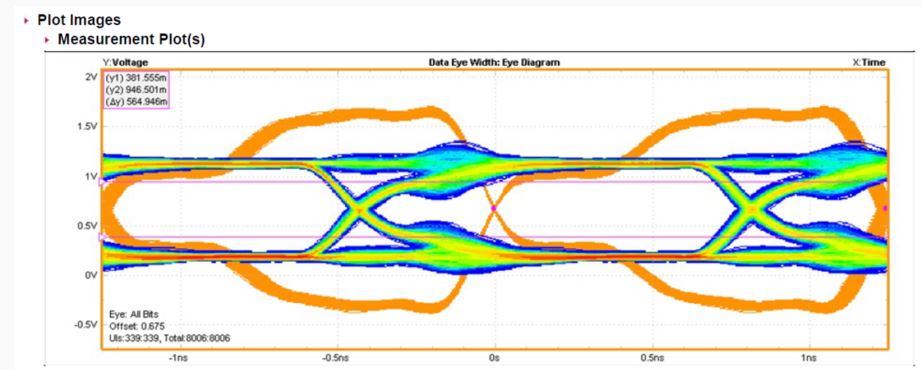
Below is a measurement of a write data eye DQS1 is orange in the back and the colored data eye is D9.
Interface voltage 1.35V
DQS1: Etch Length is 18.2mm, trace is 80 Ohm Diff
D9 : Etch length 19.3mm, trace is 40 Ohm single
I see in the AM335x errata sheet, that there is an issue with HW read / write leveling, and I also found a TI WIKI describing a procedure for SW R/W leveling.
Currently the SW loads these registers with following value.
DATAx_PHY_RD_DQS_SLAVE_RATIO = 0x38
DATAx_PHY_WR_DQS_SLAVE_RATIO = 0x35
DATAx_PHY_FIFO_WE_SLAVE_RATIO = 0x9D
DATAx_PHY_WR_DATA_SLAVE_RATIO = 0x6F
It is not clear to me if the read/write leveling only affect DDR_CLK to DQS domain, or if it also affects DQ to DQS?
Hope you can help us regarding this issue.
A couple of additional questions:
• DDR_CK = 19.11mm, DQS0 = 23.24mm, DQS1 = 18.09mm
Should PHY_INVERT_CLK_OUT be 0 or 1 in the spread sheet, when one DQS is shorter, and the other is longer than DDR_CK.?
• Is it correct that I need to modify the provided .GEL file with EMIF register values appropriate for my board, regarding ODT, drivestrengt etc.?
According to the wiki http://processors.wiki.ti.com/index.php/AM335x_DDR_PHY_register_configuration_for_DDR3_using_Software_Leveling
I need to modify DDR3_READ_LATENCY, but I cant find it in the TRM or in our code?
It is labeled “DDR2…” in the wiki but I guess that is from a older .GEL file.
For reference we are using a single DDR3 chip, Alliance AS4C128M16D3LA-12BIN
BR
Anders
Anders, can you post the RatioSeed Spreadsheet from step 2 of the above link that you referenced. Be sure to use 400MHz and PHY_INVERT_CLKOUT=1 in the spreadsheet
Because you only have one device, you shouldn't need to run the sw leveling algorithm. The results of the spreadsheet should go in this portion of the GEL file, change the red bold value to the values calculated by the spreadsheet (for PHY_WR_DATA_SLAVE_RATIO, use PHY_WR_DQS_SLAVE_RATIO + 0x40):
#define CMD_PHY_CTRL_SLAVE_RATIO 0x100
#define CMD_PHY_INVERT_CLKOUT 0x1
#define DATA_PHY_RD_DQS_SLAVE_RATIO 0x3B
#define DATA_PHY_FIFO_WE_SLAVE_RATIO 0x100 //RD DQS GATE
#define DATA_PHY_WR_DQS_SLAVE_RATIO 0x85
#define DATA_PHY_WR_DATA_SLAVE_RATIO 0xC1 //WRITE DATA
Further down in the GEL, change READ_LATENCY to CL+2
#define ALLOPP_DDR3_READ_LATENCY 0x06
Also, please post the spreadsheet from the DDR Calculation tool from step 1 of the above link you referenced
I'm not sure why the DSS script is giving you that syntax error. I will double check it on a board i have here...
Regards,
James
Anders Lange said:
Line 216 is a blank line in the script, so I don't see why that would cause an error. I'm wondering if you have an out-dated version of the script. I made a lot of improvements in recent weeks, so please make sure you have the latest:
http://git.ti.com/sitara-dss-files/am335x-dss-files/blobs/raw/master/am335x-ddr-analysis.dss
Please attach the output of the script. It provides a lot of information that might give an important clue as to what's wrong.
Brad
I still can’t run the script.
I do the following
create the .ccxml,
select segger and AM2258
save
Launch configuration
I don’t connect
View – Scripting Console
c:\ti\am335x-ddr-analysis.dss
Get a fail #102
Can you check what is going wrong:
I have attached both .DSS and the CMXL file.
I am pretty sure that I follow the README on GIT.
Can you try replacing CS_DAP_M3 on line 102 with CS_DAP_DebugSS
Thanks,
James
The issue is the Segger JTAG unit. It only supports connection to the Cortex A8 and not the DAP_M3 or the DAP_DebugSS. I will update the README to clarify on supported JTAG units.
I recommend buying a XDS110 (US $99):
http://www.ti.com/tool/TMDSEMU110-U
It will support connections to all the underlying cores which will allow all of the debug scripts to be usable.
In lieu of the dss scripts, can you provide a dump of the DDR registers 0x4c000000-0x4c000120 and you full GEL file?
Regards,
James
Hi James.
Anders, sorry, i thought you were working with GEL files. We can try to debug in u-boot, but it would be easier if they try to get the DDR stable using CCS and GEL if possible.
I'd like to focus on making sure the results of the RatioSeed spreadsheet get into the source code properly. This is important because those registers are write-only, and we cannot read them to verify the values. Below are the values from the spreadsheet that were received earlier in the thread (if these don't agree, send your RatioSeed spreadsheet). Ensure that the trace lengths are correct.
DDR clock frequency 400 MHz
PHY_INVERT_CLKOUT 1
DDR_CK trace 0.7519 0.7519
DDR_DQSx trace 0.9173 0.7165
Seed values used in CCS code
DATAx_PHY_RD DQS_SLAVE_RATIO 0x40
DATAx_PHY_FIFO_WE_SLAVE_RATIO 0xEB
DATAx_PHY_WR DQS_SLAVE_RATIO 0x7E
CMDx_PHY_CTRL_SLAVE_RATIO 0x100
If you agree with the values above, then ensure that these seed values are in the board.c file, so the ddr_data structure should look like this
static const struct ddr_data ddr3_beagleblack_data = {
.datardsratio0 = 0x40,
.datawdsratio0 = 0x7E,
.datafwsratio0 = 0xEB,
.datawrsratio0 = 0xBE //.datawdsratio + 0x40
};
static const struct cmd_control ddr3_beagleblack_cmd_ctrl_data = {
.cmd0csratio = 0x100,
.cmd0iclkout = 0,
.cmd1csratio = 0x100,
.cmd1iclkout = 0,
.cmd2csratio = 0x100,
.cmd2iclkout = 0,
};
In regards to the issues running the script, make sure the script is run after u-boot has executed. It looks like you are running it before the EMIF is configured.
Regards,
James
Hi James.
Does TI recommend trace impedance for all DDR3 lines (DQ, DQS, Address, Clk) 40 Ohm single ended and 80 Ohm diff, or 50 ohm single ended and 100 Ohm diff.
BR
Anders
Anders, we recommend 50/100. Check the datasheet, table 7-62. PCB Stackup Specifications.
Regards,
James
Hi James
Can you explain why this controller doesn’t work with 40 ohm, like other DDR3 devices?
BR
Anders
Anders, i don't know that it won't work with 40ohm, just that we recommend 50ohm. I still think the eye diagram looks very strange, since your IO voltage is 1.35V and a portion of the signal is above 1.5V. It almost seems like you have some reflections, where the first part of the eye is depressed. Can you explain why this is happening?
Regards,
James
Referring to the eye diagram is the at the bottom.
The multicolored signal is the data bit, and the single color orange, is the DQS.
The Tektronix DDRA option represents the DQS with higher amplitude.
It is a bit misleading I agree.
Here is a snip from a different design that works fine.
I am pretty sure that what we see on the current design is severe undershoot.
Anders, i looked back and it doesn't look like the debug script ran correctly. If the top of the file says "Skipping read of EMIF registers since EMIF clock disabled.", then it did not work properly. The script needs to be run when the EMIF is operational, after intialization is performed.
A couple of questions:
-you have set full thevenin for read termination. Did you try adjusting this to see if it affects the eye diagram?
-Are the IOCTRL registers set to 0x1EF? That is very high drive strength and may be contributing to your over/undershoot. Can you try adjust this back to 0x18b and see any results?
Regards,
James
-
Anders,
I'd really like to get the script working, especially since you went to the trouble and expense of buying a new emulator! It might take a few iterations, but if you'll stay with me, I'm sure we can get it shortly. I added a few additional lines to the script. Can you please re-download, re-run, and re-attach your output? We may need to do this a few times, but ultimately it will result in a more robust script for everyone.
http://git.ti.com/sitara-dss-files/am335x-dss-files/blobs/raw/master/am335x-ddr-analysis.dss
Best regards,
Brad
I had a webex and was able to get the script working. Linux was booting on the board and disabling the debug clock. From Linux console we executed the following to turn it back on:
devmem2 0x44e00414 w 0x12500002
After that, the script was able to run.