- Ask a related questionWhat is a related question?A related question is a question created from another question. When the related question is created, it will be automatically linked to the original question.

Hi .
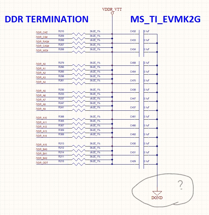
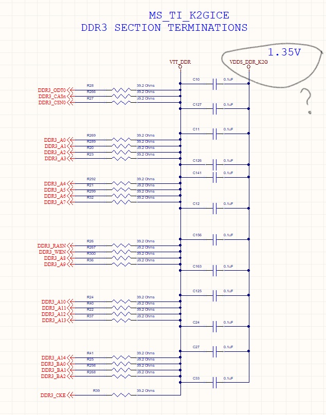
I am using "66AK2G12 "device . As two device evaluation boards are available on TI platform by Mistral solutions.
1-- MS_TI_K2GEVM
2- MS_TI_k2GICE.
There is a difference in DDR3 termination section of board interfacing with SoC. In first board capacitors terminated with "DGND"
While on other board DDR3 termination section capacitor terminated with "1.35V " net name as (VDDS_DDR_K2G).
Please someone elaborate what is difference in both techniques or which one is better.?
Schematic cutout of both are Attached below.