This thread has been locked.

If you have a related question, please click the "Ask a related question" button in the top right corner. The newly created question will be automatically linked to this question.

66AK2G12: 66AK2G12, FPGA , PCIe interface

Part Number: 66AK2G12
Other Parts Discussed in Thread: CDCM6208, TMS320C6727

Hi 

For communication between 66AK2G12 and FPGA . I want to use PCIe interface .

> Firstly is the following scheme works?

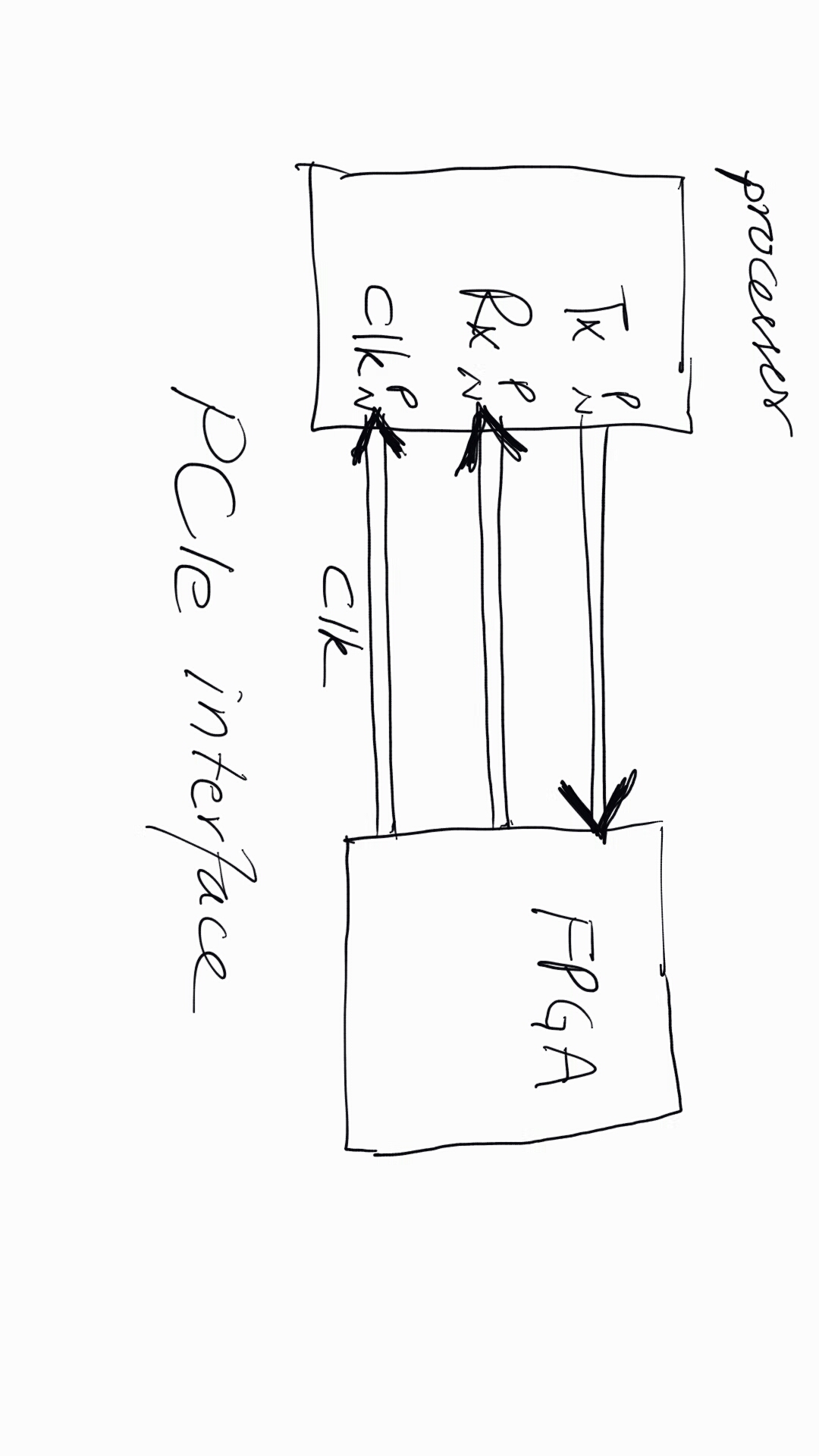
>  second issue is 66AK2G12's PCIe is at logic level of 1.8V  but FPGA bank available at 3.3V logic level. Is level shifter reliable for high speed PCIe interface.?

IF yes

please suggest some solution?

  • Hi

    Secondly FPGA build in PCI block works at 66MHz . 

    Is 66AK2G12''PCIe interface configurable for 66MHz.

    regards

  • Hello!

    The first point is about clock from FPGA towards K2 SoC, you don't really want that. Your processor device requires high quality clock to be supplied directly from clock generator or distributor. Forwarding it through FPGA is not feasible. PCIe by itself needs only reference clock, like 100MHz, though other frequencies are possible too. Then PCIe block derives its high speed clock for serial link. Note, that each receiver recovers incoming clock from data, i.e. when processors sends to FPGA, FPGA's PCIe block on receiver side recovers clock out of data. Similarly, when FPGA sends towards DSP, PCIe subsystem on processor side recovers incoming clock from serial link. Nevertheless, it is recommended that reference clock of both parties was synchronous, i.e. produced by same source.

    Second, PCIe data signals are low voltage differential, they obey different spec rather than 1.8 or 3.3 CMOS. So definitely there will be no level translators on serial link. However, FPGA needs reference clock and system reset signals, which may come at unavailable level. For reset use of level translator is recommended practice. If you don't mind share what is your FPGA maybe someone would tell more.

    Finally, 66 MHz seems unusual reference clock for PCIe, we'd better know what is that FPGA. You may want to see Figure 11-1090 in SPRUHY8H and clause 11.14.4.7 Clock Control in the same TRM.

    Hope this helps.

  • Hi again,

    I've just checked with Xilinx Artix-7, it accepts either 100 MHz of 250 MHz as reference clock, pretty much same with other Xilinx families. K2 SoC accepts only 100 MHz. So again,it looks a bit suspicious your FPGA is taking 66 MHz as reference clock.

  • Hi

    > Firstly , clock is not passing through FPGA. Although 

    PLL (phase lock loop) within FPGA  is capable of generating good quality clock (100 MHz). Which i want to use for synchronization of two devices. (DSP & FPGA).

    > Second ! ... I am using  xilinx Spartan 6  "XC6SLX150-2FGG484" FPGA  for communication with FPGA.

    > As you said " PCIe data signals are low voltage differential, they obey different spec rather than 1.8 or 3.3 CMOS" .

       But in 66AK2G12 data sheet "Table 4-1. Pin Attributes" pin I/O VOLTAGE column tells 1.8V   and  POWER column  tells PCIe interface pins at "DVDD18 / VDDAHV "


    >Thirdly ! 

    If PCIe has complexity for interfacing with FPGA  than alternatively,

    which interfaces of  "66AK2G12 " should i use for communication of DSP with FPGA .?

  • rrlagic said:

    Hi again,

    I've just checked with Xilinx Artix-7, it accepts either 100 MHz of 250 MHz as reference clock, pretty much same with other Xilinx families. K2 SoC accepts only 100 MHz. So again,it looks a bit suspicious your FPGA is taking 66 MHz as reference clock.

    Yes

    Obviously ! you  are right . FPGA not only accepts CLK upto 250MHz easily but also can easily generate clock upto 250MHz..

    > The point of 66MHz clock is Some FPGA  (i.e " spartan 6 LXT models ) has build_in IP block for PCIe interface that has limitation of 66MHz.

    but I am using XC6SLX150-2FGG484 of xilinks.

  • Hello!

    As to reference clock TRM recommends both PCIe parties clocked from same source. We have operational design where reference clocks come to FPGA and DSP from different clock generators. It's up to you to find out whether FPGA derived clock will do the job.

    You're correct that for reference clock I/O voltage is 1.8V, so if you can't match that from FPGA, that is yet another reason not to do so. Instead, you may want to use something like CDCM6208, which have controlled output voltage.

    As for reference clock speed, let me reassure you, Spartan 6 of LXT series takes reference clock of either 100MHz or 125MHz., but not 66MHz. You may confuse PCIe transaction interface in FPGA, which again runs at 62.5MHz.

    Also note, LX devices have neither PCIe hard block, nor GTP transceivers, so you can't make PCIe on LX devices. For PCIe you'll definitely need LXT device.

    Considering alternatives to PCIe keep in mind, that PCIe is designed to provide addressing. You may opt for Gigabit Ethernet, however, it this case packetising and addressing will be your job. There is no Ethernet in LX devices.

    There is yet another alternative as GPMC. With it you may have parallel type of interface, which probably is the easiest thing, but it is no way high speed interface. We know nothing about your target application, and device you selected for FPGA is again a bit confusing. On one hand, it's a largest 150K cell device, on another - it is in rather small 484 package. So you have to check whether you have enough pins to implement parallel interface. Keep in mind, GPMC is just 16-bit wide.

  • HI 

    thanks  a lot for recommendation about interfacing.

    > In my previous version of board, i had used DSP (TMS320C6727)' EMIF interface for communication with FPGA  (XC6SLX150-2FGG484 ).Which is working well.

    > That why in my next version of board i want to upgrade my processors resources " thats why i choose 66AK2G12" s EMIF interface for the same FPGA.

    > But after much of work done on board this EMIF interface can only works with memory  not with FPGA. thats why i  want to add  some other interfaces for data communication between devices.

    > Second option is PCIe and Ethernet   , which has no support on LX device. 

    > Now i want to make this board functional by adding some alternate interfaces between FPGA and DSP.  like GPMC or any other interface possible like else.

    >Hopefully  in next version of board ,i replace LX device with LXT device for enhancing board interfacing performance.  

    > Now i added "GPMC" interface between devices for communication.  

    which should i add as backup of GPMC between 66AK2G12 and FPGA. like SPI .Data rate bandwidth does not matter now.