This thread has been locked.

If you have a related question, please click the "Ask a related question" button in the top right corner. The newly created question will be automatically linked to this question.

[FAQ] PRU: How do I calculate read and write latencies?

Part Number: AM6442

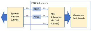
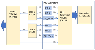
I am writing a PRU application for a PRU-ICSS device (AM335x, AM437x, AM57x), PRU-SS device (AM62x), or a PRU_ICSSG device (AM24x, AM64x, AM65x). I want to calculate how many clock cycles a read or a write will take. How do I do it?

This FAQ is an extension of the PRU Read Latencies app note. The app note will be updated with information from this FAQ at a later point in time.

  • PRU Read & Write Instructions 

    Processor cores work by executing instructions. Even if the PRU firmware is programmed in C, the C compiler will convert the C code into instructions that the PRU cores can run. PRU firmware can also be written in assembly in order to directly control every single instruction that runs on the PRU cores. If the application cares about whether a read executes in 6 PRU clock cycles or 7 PRU clock cycles, the time sensitive code should probably be written in assembly.

    This document will use the term "latency" to describe the time it takes for an instruction to execute.

    The full PRU instruction set is documented in the PRU Assembly Instruction User Guide. That document lists three kinds of read & write instructions:

    LBBO (load byte burst) & SBBO (store byte burst) 

    LBBO and SBBO are the default read (i.e., load) and write (i.e., store) PRU instructions. This FAQ will focus on calculating read and write latencies with LBBO and SBBO.

    LBCO (Load Byte Burst with Constant Table Offset) & SBCO (Store Byte Burst with Constant Table Offset) 

    LBCO and SBCO work similarly to LBBO and SBBO. However, instead of using a register to specify the read/write memory address, LBCO and SBCO use an address from the PRU Constant Table. The latency for LBCO and SBCO to execute is the same as the latency for LBBO and SBBO.

    While the latency to execute just the read or write is the same, LBCO/SBCO take fewer clock cycles overall. Since the read/write address for LBBO/SBBO is stored in a register, LBBO/SBBO require additional assembly instructions to load the address into the register. Since LBCO and SBCO use a constant table entry for the read/write address instead of a register value, LBCO and SBCO do not require the additional "address load" assembly instructions.

    Broadside commands: XIN (Register Transfer In), XOUT (Register Transfer Out), XCHG (Register Exchange)

    TODO: is XCHG supported for PRU_ICSSG devices? The assembly instruction user guide indicates XCHG is not supported for AM335x

    XIN & XOUT can be used to read or write up to 31 registers to or from a broadside interface. Since XIN & XOUT execute in a single PRU clock cycle, they are the fastest way to move data. However, XIN and XOUT can only communicate with modules that are attached to that broadside interface.

    Different PRU devices have different broadside interface attachments. For example, AM335x can use XIN & XOUT to move registers between the PRU core and scratchpad registers, or directly from one PRU core to the other. AM64x can use XIN & XOUT to move information to and from scratchpad registers, but NOT directly to another PRU_ICSSG core. However, AM64x can ALSO use XIN & XOUT to access its own dedicated broadside (BS) RAM, or to read & write multiple registers to a memory space outside of the PRU_ICSSG through the XFR2VBUSP interface. For more information, please reference the Technical Reference Manual (TRM) for the desired processor.

    Broadside commands will not be discussed in this FAQ.

  • How do I tell if a read or write is deterministic? 

    PRU cores are completely deterministic. That means we can know exactly how long every PRU instruction will take to execute... with some exceptions, which are described below. 

    Non-read & write instructions 

    PRU instructions that are not reads or writes are completely deterministic. These instructions will always take exactly one PRU clock cycle to execute.

    Read & write instructions to an address within the PRU Subsystem 

    Reads and writes to an address within the PRU subsystem are completely deterministic. However, there is some extra math involved:

    There are specific rules for how long a read or a write instruction will take. We will cover those rules in depth below.

    But what if a PRU core is trying to access a peripheral within the PRU subsystem, and another core is already reading or writing to that peripheral? Or what if two cores try to access the same peripheral on the exact same clock cycle? Only one of the cores can access the peripheral at a time, so the PRU subsystem arbitrates between the two cores to decide which core gets to go first. Once one core is reading or writing to the peripheral, then the second core will stall until the peripheral becomes available. The stall time is called "arbitration delay".

    When designing a PRU system with sensitive timing, the designer must keep in mind the lowest possible delay (i.e., "time to do the read/write"), and the highest possible delay (i.e., "time to do the read/write" + "arbitration delay").

    Read & write instructions to a system address outside the PRU Subsystem 

    Reads and writes to addresses outside of the PRU subsystem are NOT deterministic. There may be choke points, arbitration delay, impacts from other cores, etc. However, you can still approximate the latency of external reads and writes by performing tests.

    PRU-ICSS cores and PRU-SS cores will not experience arbitration delay when the signals exit the PRU Subsystem (though the LBBO commands may still be impacted by arbitration delay in other parts of the system). However, PRU_ICSSG accesses to the external system must take arbitration delays into account.

  • Calculating write latencies with SBBO 

    PRU-ICSS / PRU-SS Write to memory locations outside of the PRU subsystem: N PRU clocks to write N words

    These instructions are fire-and-forget.

    There are buffers between the PRU subsystem and the rest of the device. It takes N clock cycles for SBBO to write N words to the system bus buffer. Then the PRU will move to the next assembly command without waiting for the write to complete. It will take additional time for the value written to the buffer to travel through the system busses and eventually update the external memory address.

    This assumes that the SBBO writes are to addresses that are word aligned (e.g., 0x100, 0x104, 0x108, etc). Whenever the load crosses a 4 byte boundary, it takes another PRU clock cycle.
       - e.g., write 2 bytes to 0x100: one PRU clock
       - e.g., write 2 bytes to 0x102: one PRU clock
       - e.g., write 2 bytes to 0x103: two PRU clocks (one clock to write to the word at 0x100, one clock to write to the word at 0x104)
     * Thus, if the write address is not word aligned, the equation changes to N + 1 PRU clocks for SBBO to write N 32-bit words

    PRU_ICSSG Write to memory locations outside of the PRU subsystem: N PRU clocks to write N words, plus per-slice arbitration delay 

    See the PRU-ICSS / PRU-SS section above, and the arbitration delay sections below.

    PRU-ICSS / PRU-SS Write to memory locations within the PRU subsystem: N PRU clocks to write N words, plus arbitration delay

    There are no buffers between the PRU core and memory internal to the PRU subsystem. Thus, if another core is using an endpoint connected to the ICSS CBASS bus, the PRU core has to wait for the endpoint to become available before it can perform a write.

    The internal CBASS interconnect is "fully switched". That means that multiple cores can use the CBASS simultaneously, as long as the cores are accessing different endpoints. e.g., PRU0 can access DRAM at the same time that PRU1 is accessing the PRU's hardware UART.

    See the "deep dive on arbitration delay" section below for information on how to calculate arbitration delay.

    The same word alignment rules apply here. i.e., if the write is not word aligned, add 1 additional clock cycle.

    PRU_ICSSG Write to memory locations within the PRU subsystem: N PRU clocks to write N words, plus arbitration delay 

    See the PRU-ICSS / PRU-SS section above. Note that there is one single internal CBASS per ICSSG. So cores that are in different slices will still deal with arbitration delay if they are trying to access the same endpoint at the same time.

  • Calculating read latencies with LBBO 

    PRU-ICSS / PRU-SS Read: Read instructions will take multiple PRU clock cycles, depending on how far away the destination address is on the processor. Reads from memory locations within the PRU subsystem may have arbitration delay.

    See the "deep dive on LBBO & DRAM" section below.

    The same word alignment rules from SBBO apply here. i.e., if the read is not word aligned, add 1 additional clock cycle.

    PRU_ICSSG Read: Read instructions will take multiple PRU clock cycles, depending on how far away the destination address is on the processor. Reads from memory locations within the PRU subsystem may have arbitration delay. Reads from memory locations outside the PRU subsystem may have per-slice arbitration delay

    See the arbitration delay sections below.

    Deep dive on LBBO & DRAM 

    LBBO from PRU DRAM takes 2 + N PRU clocks to read N words (plus arbitration delay, plus 1 PRU clock if address is not word aligned)

    LBBO takes 3 clock cycles to get the first 4 bytes of data from PRU internal memory. Every additional 4 bytes adds 1 clock.

    for example,  LBBO loadDestination, loadAddress, 0, 16
    takes 6 PRU clocks: 3 clocks to load the first 4 Bytes, and 3 clocks to load the next 12 Bytes

  • Arbitration delay & PRU Bus Structure

    PRU Bus Structure: PRU-ICSS, PRU-SS

    The PRU subsystem has an internal CBASS (also called VBUSM). Each PRU core has a direct connection to the internal CBASS, and to the system CBASS. Accesses to the external CBASS are totally separate from accesses to the internal CBASS. That means that reads or writes over the internal CBASS are unaffected by reads or writes over the external CBASS.

    VBUSM interconnects are "fully switched". That means that multiple cores can use the CBASS simultaneously, as long as the cores are accessing different endpoints. e.g., PRU0 can access DRAM at the same time that PRU1 is accessing the PRU's hardware UART. An endpoint can be a peripheral, or a memory. Separate memories act as separate endpoints (e.g., one core can access DMEM0, one core can access DMEM1, and another core could access SRAM simultaneously).

    PRU Bus Structure: PRU_ICSSG

    In addition to the CBASS interfaces on PRU-ICSS, the PRU_ICSSG has a VBUSP between each ICSSG slice and the external CBASS. VBUSP is different from VBUSM, because VBUSP can only be used by one core at a time.

    Arbitration on the internal CBASS

    Any time a PRU core performs a load or store (i.e., read or write) from an endpoint in the internal CBASS, there is a chance that another core is already accessing that endpoint.

    The internal CBASS bus is 4 Bytes wide. This applies to all PRU devices. So if another core is performing an atomic write of x Bytes then it will take ceil(x/4) PRU clocks for the write to occur. E.g., a write of 30 bytes would take ceil(30/4) = ceil(7.5) = 8 PRU clocks to complete.

    If a PRU core and a non-PRU core (e.g., Linux A53 or RTOS R5) try to access the same PRU Subsystem location during the same PRU clock cycle (SRAM, UART, ECAP, etc), the PRU wins. However, if PRU initiates a transaction from SRAM after another core is executing a burst write transaction, the PRU transaction will stall until the burst write is completed. So if the non-PRU core's write takes 8 PRU clocks to complete, the longest the PRU would have to wait is 8 - 1 = 7 PRU clocks. If you want to completely avoid arbitration delay, you could program the non-PRU core to perform multiple 4 Byte writes instead of a single long write. In that case, the PRU would win arbitration every clock cycle it initiates a read.

    PRU-ICSS, PRU-SS: If two PRU cores try to access the same PRU subsystem location during the same PRU clock cycle, then PRU0 wins (except for DMEM1, where PRU1 wins).

    PRU_ICSSG: If multiple cores try to access the same PRU subsystem location during the same PRU clock cycle, then the core with higher priority wins. The cores are listed in order of highest to lowest priority: PRU_TX0 > PRU_TX1 > PRU0 > PRU1 > RTU0 > RTU1.

    Arbitration to the external CBASS (PRU_ICSSG only)

    PRU-ICSS & PRU-SS cores will not experience arbitration delay when trying to access the external system CBASS.

    Each PRU_ICSSG slice has a choke point where the PRU, RTU, and TX_PRU all connect to the same VBUSP, which connects to the external CBASS. Thus, if one core in a slice is reading or writing to the external CBASS through the VBUSP, the other cores in the slice cannot access the external CBASS until the VBUSP becomes available. The interface to the external CBASS is 4 Bytes wide, so the math to calculate arbitration delays to the external CBASS is the same as calculating arbitration delays to the internal CBASS. See the "internal CBASS" discussion of arbitration delay for how to calculate the arbitration delay for an atomic read or write.

    If multiple PRU_ICSSG cores try to access the external CBASS at exactly the same clock cycle, arbitration priority is: TX_PRU first, then PRU, then RTU.

    There is NOT a choke point across slices. e.g., if ICSSG1_PRU0 is using the external CBASS, then ICSSG1_PRU1 is NOT affected by arbitration delay since it is in a separate slice.