This thread has been locked.
If you have a related question, please click the "Ask a related question" button in the top right corner. The newly created question will be automatically linked to this question.
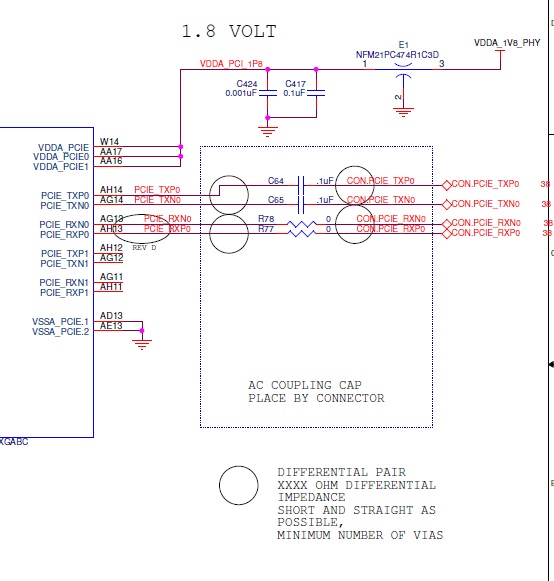
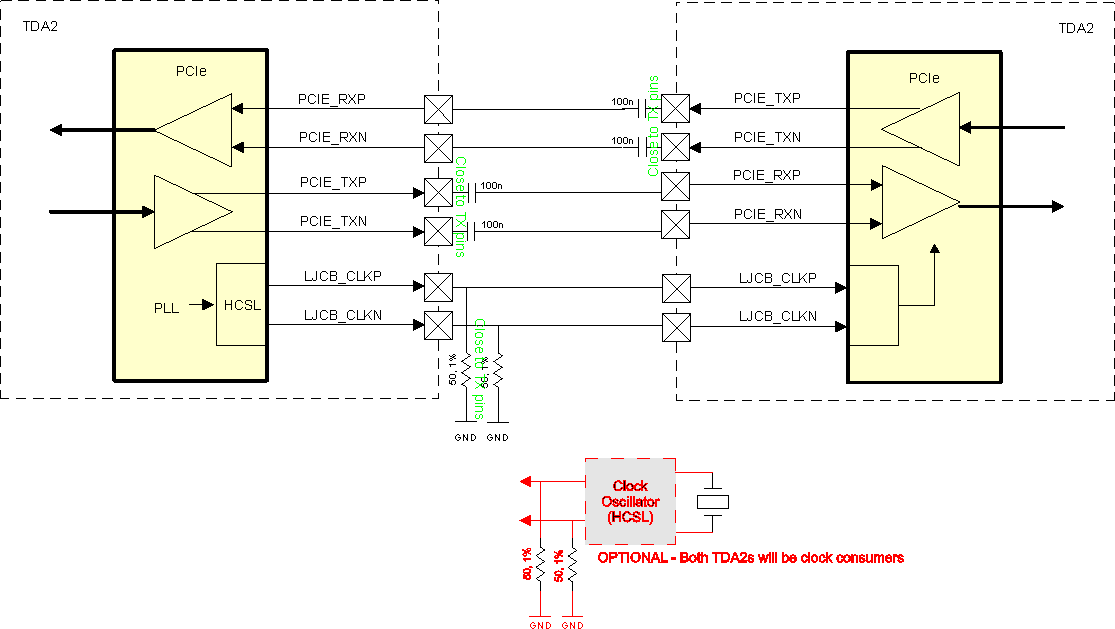
Is the a requirement for termination resistors on TX and RX for the PCI-e layout?
This PCI-e bus is chip to chip not to an off board device.
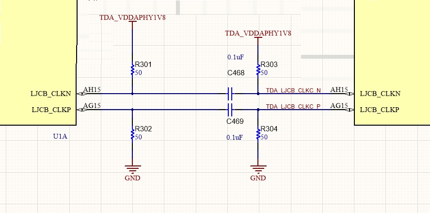
I see in the recommended layout details for differential and single ended trace impedance. The is detail on the clock termination 50 ohm to GND on P and N. Other resources for PCI-e show TX and RX termination resistors both to GND and across P and N.
Hi,
Can you please post a diagram of the clocking? Including the clock generator IC, clock path, clock inputs of TDA2s.
Thanks,
Stan
Hi Zach,
This must be like bullet (1) from my previous post.
Assuming U1A is clock source and the other TDA2 is clock consumer, then you need only R301 and R302. Other components must be removed.
Regards,
Stan
Stan,
Ok. Remove the capacitors as well so not AC coupled as I read in the datasheet.
So my original question, the TX and RX signals. These do need to be AC coupled and don't need termination resistor just the impedance controlled trace?
Thanks,
Zach