This thread has been locked.

If you have a related question, please click the "Ask a related question" button in the top right corner. The newly created question will be automatically linked to this question.

AM5716: GMPC - AAD mode

Part Number: AM5716

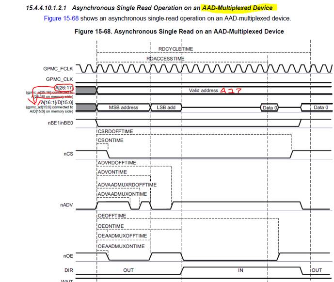
Our AM5716 application will use the GPMC parallel bus as “Multiplexed 16b NOR type” in AAD (address-address-data) mode.  Does this arrangement provide all [27:1] address bits?  That is,  when A[MAX:17], A[16:1] D[15:0] are sequentially multiplexed onto the gpmc_ad[15:0] pins, what’s the numerical value of ‘MAX’?

The TRM timing diagrams for AAD mode show address line usage for AD mode so it’s not clear just what AAD mode address range is.

  • Hello,

    Is there any update on this? We have some further questions:

    1. We have these hw devices on the GPMC pins:

    1. eMMC on MMC2 (for primary boot)
    2. SD card on MMC1 (for development boot)
    3. PLD on GPMC (PLD acts as bridge to several parallel bus devices, emulates “Mux’d 16b NOR type – Synchronous” interface.  No boot.)

    These all seem to fit using the PinMux tool.  Are they all compatible with each other?   

    2. The PinMux tool doesn’t differentiate between ad and aad mux mode for the GPMC.  Am I setting it up right for aad mode?  I have a[10:1] not connected.

    3. What address signals are active in the MSB (first word of aad sequence)?  Is a27 active on its own pin in aad mode?

    4. Any advice on how to set the GPMC clock to our preferred frequency (54 MHz) without upsetting some other module’s clock?  The CTT shows what can change, but I haven’t figured out how to determine if there are undesired results from the changes I enter. 

    5. In the device tree, how is the GPMC set up for the way we’re using it?

    I can send over the pinmux output file if needed.

  • Nicholas,

    For AAD-pin usage, please reference Table 15-438 of the AM571x TRM.  It has a detailed view of what pins are available under multiplexed & non-multiplexed settings.  Yes all A[1:27] will be accessible.

    1 & 2. For concurrent operations with MMC2, MMC1, and GPMC, since MMC2 signals are MUX'd on GPMC signal lanes, you will have to multiplex some of the GPMC functionalities on other signal lanes for proper functionality.  Any incompatibility should be specified by the PinMux Tool; you can also sanity check to make sure the overlapped signals (GPMC_A27, CS1) are mapped somewhere else.  Please make sure you implement the correct pulls based on device specifications.

    3. In AAD mode, GPMC_A[17:26] are mapped onto GPMC_A[1:10], so you should have these pins connected.  GPMC_A[11:26] are not used for AAD, but you will need some of them for MMC2 connections.

    4. GPMC FCLK comes from L3INIT_L3_GICLK on DPLL_CORE, therefore any changes will also impact MMC1/2, USB, and SATA, and you will have to analyze if the changes will cause issues with the other peripherals.  The CCT is the best resource for recommending the values to set; remember you also have the option to leverage GPMC_CONFIG1_i[1:0] GPMCFCLKDIVIDER to change only the GPMC interface clock.  Any reason why 54 MHz is needed?

    5. Please clarify your question in device tree.  Are you referencing GLSDK or Android?  u-boot or kernel?

    Have a great day!

    Best Regards,

    Shiou Mei

  • Hi Shiou,

    #1 & #2: we're good here

    #4: is a left over from a previous design, so this will be removed 

    #5: TBD, still looking into this. 

    #0:

    Table 15-438 does not show AAD mode.  It does show AD (‘Multiplexed Address Data’) mode, which uses gpmc_a[10:1].  AAD mode uses only the data bus (ad[15:0]) for address and data.

    #3:

    I think the response is wrong.  I think gpmc_a[10:1] pins are not used in aad mode, and A[17:26] are instead mapped onto ad[15:0].  TRM describes AAD mode:

    For an AAD-multiplexed access, all address bits are passed onto the data bus using two nADV rising edges. The first rising edge latches the address most-significant bit (MSB) down to bit 17, while the second rising edge latches address bits 16 down to 1 (TRM section 15.4.4.7, last paragraph).  So only the data bus, ad[15:0], pins are used.  This also correlates with what I see on NOR flash specs that support AAD.

    Adding to the confusion, all the cycle timing diagrams for AAD mode in the TRM show similar error, which I think could be corrected thus:

    Thanks,

    Nick

  • Nick,

    Thank you for catching me!  I was typing AAD-multiplexed in my responses but I was thinking AD-multiplexed the entire time.  I checked into the spec and yes you are correct addresses are all multiplexed onto the DAT line.  However, according to the spec, the multiplexed addresses are A[27:17] during the first MSB transfer, and then A[16:1] during the second LSB transfer.  None of the GPMC_A[27:0] lines should be connected externally in AAD-multiplexed mode, though they should still still retain valid value, and have their values passed onto the DAT bus via nADV signal.  Updated diagram below:

    Please confirm this updated diagram matches the expected behavior of the NOR flash spec you have.  It would be great if you can share the AAD-capable NOR flash spec as well so I can use for future reference.

    Have a great day!

    Best Regards,

    Shiou Mei

  • Hey Shiou,

    Thanks for the quick reply! The image you attached ran into an error, can you reattach it?

    Thanks,

    Nick

  • Nick,

    See attached.

    Best Regards,

    Shiou Mei

  • Sent over email, Thanks for the help!