This thread has been locked.

If you have a related question, please click the "Ask a related question" button in the top right corner. The newly created question will be automatically linked to this question.

AM3874: Boot-behavior and clock subsystem (pcie / serdes)

Part Number: AM3874
Other Parts Discussed in Thread: CDCM61002

We are using the Sitara AM3874 and have some questions regarding the boot-behavior and the clock subsystem. Some boards behave in another way than others with the same hardware and software version.

In our system we are using a clock generator (TI CDCM61002) for the SERDES_CLK and PCIe_CLK. The input-reset of the CDCM is the output-reset (RSTOUT_WD_OUT) of the AM3874, only connected to a pull-up.

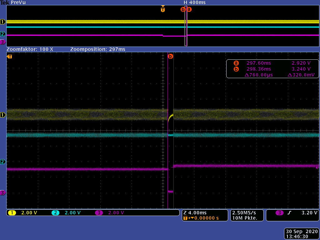
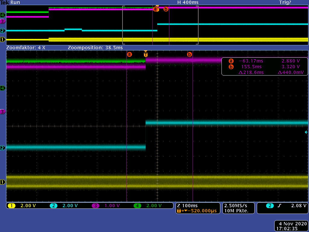
Comparing to boards we see that the RSTOUT_WD_OUT goes low (0V) on board 1, but on board 2 the signal on goes down to about 2.8V.

Another interesting difference between the two boards is the behaviour of PCIe_clk when only the supply of the CDCM is stable and the other supplies for the ARM are ramping up. On board 2 the pcie and serdes_clk are running and on board 1 after nPOR is released.

Question: Why are there such difference?

As described in sprugz7e 2.7.11 (and in sprs695c) the RSTOUT_WD_OUT is optional, depending on the BTMODE[11]. This BTMODE is latched when nPOR is de-asserted. We tried to change the PD/PU resistor on gpmc_ad[11], but it has no effect. 

Regarding the PORz Sequence the external clocks must be stable before POR is released. As described above on board 1 the RSTOUT_WD_OUT is low -> the serdes_clk and pci_clk are also low. So the point 7 in chapter 2.7.15 “When power and clocks to the chip are stable, PORz is de-asserted” cannot be reached.

We see the internal pll don’t lock, so we have startup problems.

Question: How is it possible to disable the RSTOUT_WD_OUT assertion during an active POR ?

Edit (09/23/2020):

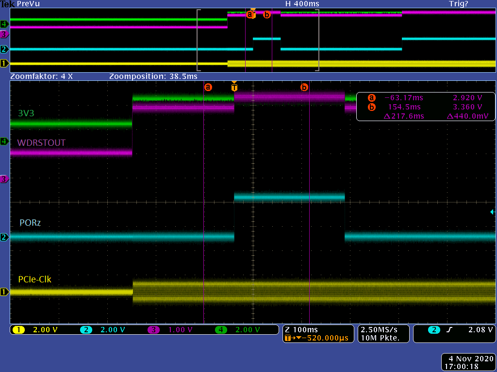
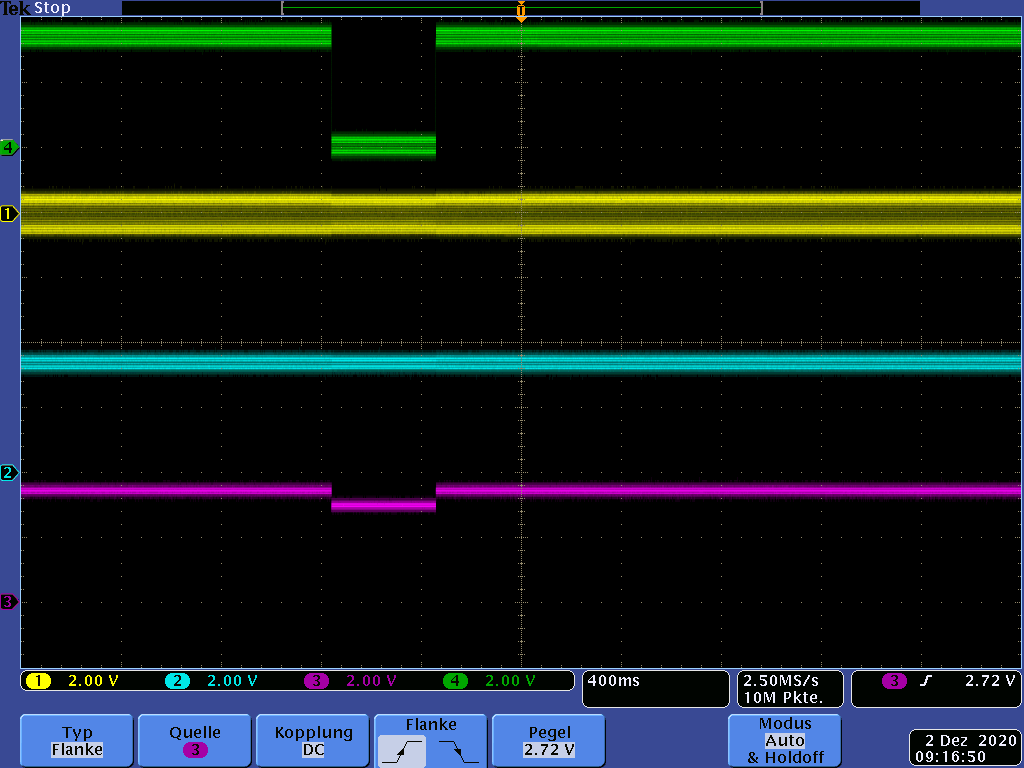
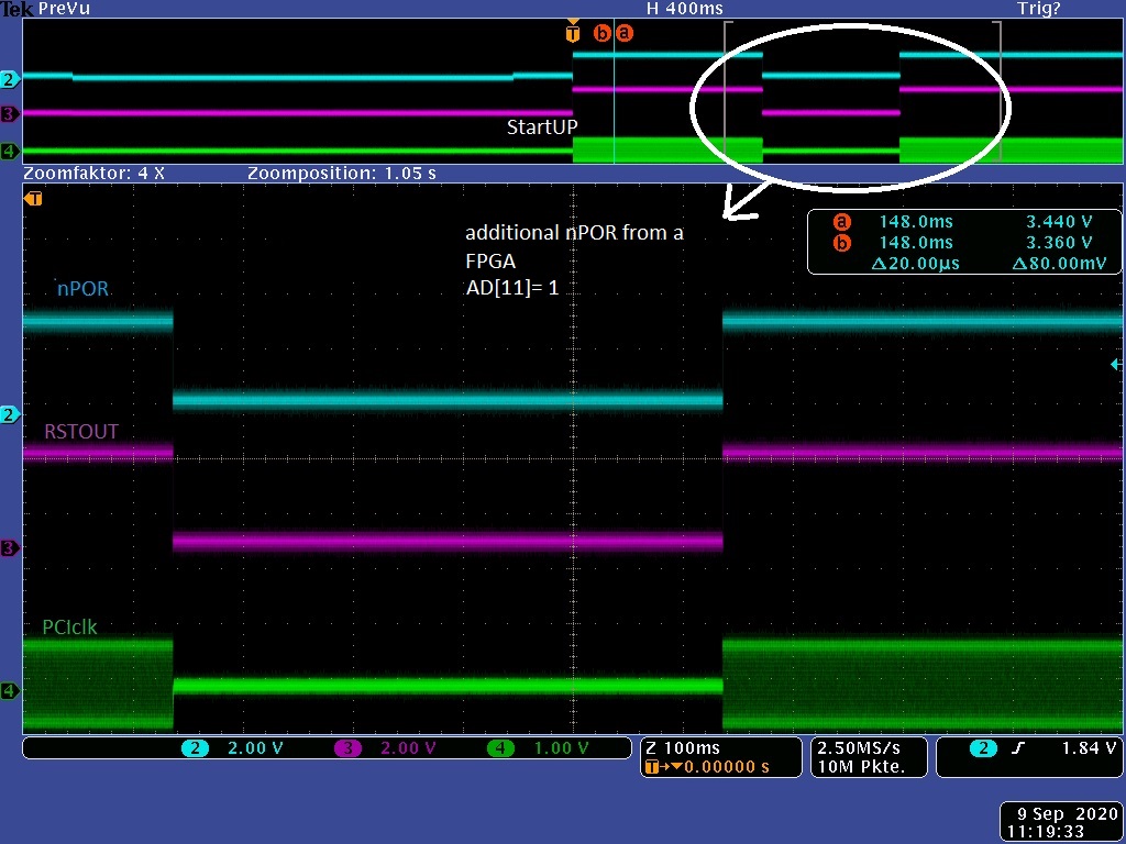
This is the behavior of the device 1. The trigger postition is about power on. We added a POR-Sequence from a connected FPGA, which also can control the signals POR, RESET(in) and GPMC_AD[*], We forced the gpmc_ad[11] to '1' until the por-signal deasserts.

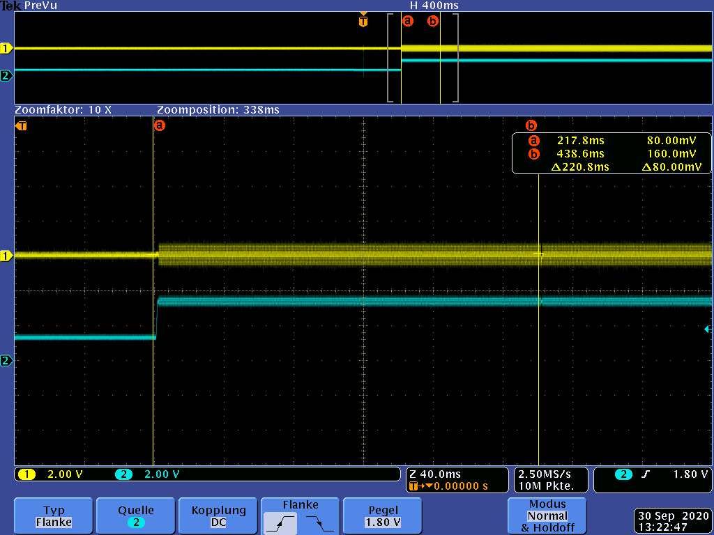
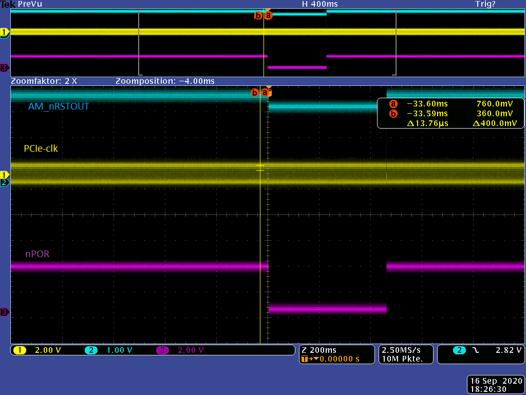
For comparision the device 2 - as you can see there is only a 0.5V-drop on the signal WD_RSTOUT (this is very confusing).

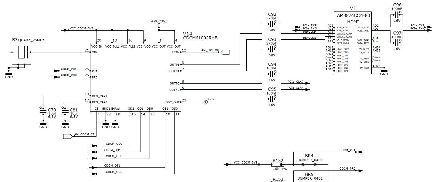
The following schematics-parts are showing the connection of the described clocks and Reset-Signal.

  • Hi Chris,

    Which OS are you using?

  • Hi Chris, the fact that RSTOUT_WD_OUT is inconsistent across boards implies that there is something wrong with the power sequencing, reset, or boot pin latching.  First, check the POR vs the power sequencing and ensure that none of the timing is violated from the datasheet Figure 8-1.  Also, the reset timing described in section 8.3.2 should also be followed.  You should also check to ensure the boot pins BTMODE are stable around POR deassertion.  If you have JTAG, you can check how the boot pins were latched by checking the CONTROL_STATUS register.  Check this register after several boots on both boards to ensure the same value is getting latched.  Also ensure the external warm reset signal RESET is stable and not attempting to reset the device.

    Regards,

    james

  • Hi,

    this behavior is independent from our OS. In the observed time where the problems the uboot is still active. We see the resulting problem in Linux as well in CE

  • Hi James,

    thanks for your quick answer. I edited the post with addtional screenshots.

    The power sequencing was checked by TI serveal years ago and should be within the specification. As a "cross-check" we added a POR about 500ms after PowerUp. The AD-Signals are forced to the desired value (e.g. gpmc_ad[11]='1'), reset_input was high (warm reset), nPOR was low. (nPOR=0 & reset_input=0 has the same behavior).

    We also scoped the setting with gpmc_ad[11]=0 and we see the same behavior. (current setting by PU/PD).

    We dump the value of the CONTROL_STATUS register in the boot-sequence and both devices are having always the "boot-code".

    Regards

    Chris

  • Is RSTOUT connected to anything else, other than what is shown in the schematic?  Can you check DVDD, which is the IO voltage for the pin, around the point where RSTOUT is 2.8V.  Have you considered that there may be an assembly issue on board 2?  Is there a 3rd board you can compare to?  The function of RSTOUT is fairly simple, so the fact that it is acting strange doesn't make sense, points to maybe a power supply issue. I would check the power rails on board 2 specifically.

    Regards,

    James     

  • JJD said:
    Is RSTOUT connected to anything else, other than what is shown in the schematic? 

    No, there is no other part included.

    JJD said:
    Can you check DVDD, which is the IO voltage for the pin, around the point where RSTOUT is 2.8V. 

    The VCC3V3 is completly stable all the time.

    JJD said:
    Have you considered that there may be an assembly issue on board 2?

    We don`t see an assembly problem on board 2. This board is tested from our partner (AOI, voltage tests, software is running and so on).

    JJD said:
    Is there a 3rd board you can compare to? 

    I saw the same behavior of board 2 on another board.

    We are checking some other boards at the moment, so we will get an better overview how the boards behave.

    Do you have further suggestion we can focus on in the tests (exept the power rails)?

    Thanks

    Chris

  • Hi Chris, thanks for the responses.  I'm still perplexed by the behavior of RSTOUT_WD_OUT signal.  In the TRM, is specifically states in table 8-8:

    While POR and/or RESET is asserted, the RSTOUT_WD_OUT pin is 3-stated and the internal pull resistor is disabled; therefore, an
    external pullup/pulldown can be used to set the state of this pin (high/low) while POR and/or RESET is asserted. 

    This completely contradicts what i see in your scope shot, as RSTOUT_WD_OUT should be high with your external pull up.  Is the scope shot the first time PORz is asserted?  Or is PORz controlled by some other mechanism.  The scope shot implies that a previous PORz occurred, and BTMODE[11] was latched as a 0 at that time.  I think I would like to see a scope shot of the first porz along with supplies and RSTOUT.  It seems like there may be some issue with this initial power up sequence, which needs should look more like figure 8-1 and figure 8-4 in the datasheet

    Regards,

    James   

  • Hi James,

    the answer is late because I was on vacation.

    In the meantime a collegue of mine has done some measurements with 3 other boards and they behave like device 2.

    As you can see, that the RSTOUT_WD_OUT is 2.9V in that device. We also see a little drop to low, this could be the release of nPOR and latch the BTMODE[11], this is 0 on this board. We will crosscheck the behaviour of this drop, when BTMODE[11]=1.

    The next screenshot shows the startup of the device. The blue line is the vcc. The PORz is released about 200ms after stable vcc, so the pcie-clk starts to run with stable voltage.

    JJD said:
    Or is PORz controlled by some other mechanism.

    The PORz is controlled by 2 devices. The first one releases the PORz when the voltages are stable (~200ms) and we can control the PORz with a FPGA for a reboot-sequence on a running device.

    JJD said:
    figure 8-1 and figure 8-4 in the datasheet

    Do you refer on the document "SPRS695D"? We checked the OPP-voltage and it looks good.

    We are having an additional question which (maybe) corresponds with that. We see on the same board "good and bad boots". In the case of a bad boot, the system crashes when we want to access an PCI-register:

       Start of PCIe link training sequence ...
            READ REGISTERR pDev->PCIESS + SPACE0_LOCAL_CFG_OFFSET + DEBUG

    In a "good boot" we see:

    Start of PCIe link training sequence ...
    READ REGISTERR pDev->PCIESS + SPACE0_LOCAL_CFG_OFFSET + DEBUG    PCIe LTSSM state: 0x00 -> DETECT_QUIET
    Initiate Link Training
    READ REGISTERR pDev->PCIESS + SPACE0_LOCAL_CFG_OFFSET + DEBUG    PCIe LTSSM state: 0x01 -> DETECT_ACT
    READ REGISTERR pDev->PCIESS + SPACE0_LOCAL_CFG_OFFSET + DEBUG    PCIe LTSSM state: 0x11 -> L0
    Link Training succeeded in 14 ms, LTSSM state: 0x11

    Thanks and regard

  • If you are getting good and bad boots on the same board, something is probably marginal in the power up sequencing.  I still would suggest to probe the signals in figure 8-1 and 8-4 in the datasheet to see if the timing matches the diagrams.   Also, you should be getting the correct voltages on the signals based on your IO supply voltages.  If not, there is probably some contention on the signal which needs to be resolved, or maybe there is an issue with the supply

    Regards,

    James  

  • Hello James,

    first of all, we hope we can explain the good and bad boots and may have a solution, which must be proven. In a screenshot above you can see a little drop of the RSTOUT. This RSTOUT resets the PCIe-clk for about 760µs, but the pll for the clock looks before. So it seems to be random, if the clock is on the same phase.

    We can set the BTMODE[11]=1 and so this drop doesn´t occur in device 2, but

    1. we cannot explain the voltage drop to 2.9V, when PORz is asserted. You said, that the signal is 3-state in that moment.

    2. we have some boards where the drop is to 2.9V and some boards (e.g. device 1) it drops down to 0.5V. But we don`t have seen a board with a 3.3V-level yet.

    So that means in case 1, the RSTOUT-signal is good enough to be a high-level on the clock generator and in case 2 the signal causes a clock-reset.

    We heated and cooled the ARM-CPU and the voltage-level differs in both devices by about +/- 100mV. This is not what we expect, when the signal is 3-stated from internal. We have an external pullup by 4.75k and an internal pullup in the CDCM61002 with typically 150kOhm. It seems that there is an active pulldown in the CPU.

    We also measured the voltage during the PORz, there are all stable and within the specified range. It also makes no difference, if the PORz is coming from a power cycle or if we assert the PORz during the normal operational mode.

    Regards

    Chris

  • Chris, can you perform the following test:

    -Record registers CONTROL_STATUS, BOOTSTAT, and PINCNTL262.  Then assert PORz. and check the voltage on RSTOUT signal

    Keep doing this until until you see

    a) 2.9V on RSTOUT

    b) 0.5V on RSTOUT

    I'm trying to see in each case what the latched boot mode is and the corresponding behavior, along with the pull configuration on that signal.   The datasheet indicates that the RSTOUT is 3-state during POR or RESET assertion at first power up, but subsequent assertions of POR or RESET will assert RSTOUT_WD_OUT if BTMODE11 was latched as 0  

    My theory is that when you see 2.9V, BTMODE11 was latched as 1 and the pull down on RSTOUT is enabled, and when you see 0.5V, BTMODE11 was latched as 0 and RSTOUT is being driven low

    Regards,

    James

    Regards,

    James

  • Hello James,

    thanks for the ideas, but unfortunately there is no change in the behaviour of the boards. We forced the PORz-signal with an additional and switchable pull-down, so had varied the deassertation of this signal, independent from the power-up chip.

    We see in our boot-log, that the BTMODE[11] is set to 0 or 1 - depending on the time-position of the latch.

    On the observed board the level during low-active PORz is always about 2.9V.

    This is a normal power-up (without additonal PORz-pd). The second PORz-assertion is done via a FPGA.

    The release of the pulldown of PORz is done after about one second, so the BTMODE[11] should be stable.

    The level 2.9V of the WDRSTOUT is also directly after PowerUP, where the PORz is low.

  • Hello,

    Sorry for the delay in response.  This case has been transferred to me and a colleague (Brad) going forward.  (I'll admit I haven't completely digested the different permutations of boards and experiments, but it does clearly seem that this isn't behaving as stated in the data sheet)

    I have come across an old thread that suggests RSTOUT_WD_OUT is actually asserted/driven (not high-z) during PORz.

    I have a couple of suggestions/guesses.

    -1- Can you remove the CDC device from one of your systems to make sure there isn't some weird contention occurring?

    -2- The datasheet states that BOOTMD pins are latched when PORz is deserted.  And it does seem the bootmd[11] signal has some effect in the 2.9V case based on the 760 us assertion of the RSTOUT_WD_OUT.  

    One theory is that the the bootmd[11] internal logic may default  to a random state during initial power-up and when PORz is asserted.  If that were the case, it could result in sometimes driving high (2.9V) and sometimes driving low (0.5V).  (based on the idea that it doesn't go high-z as per the other e2e thread)

    Can you run an experiment where you power-up as normal (and instead of your experiment where your FPGA drives PORz a 2nd time) can you drive RESETn active for a second time?  And experiment with BTMODE[11] at 0 and 1.

    Thanks,

    Kyle

  • Looking at the CDCM61002 datasheet it says:

    "For proper device operation, the reference input must be stable at the start of VCO calibration. Since inputs from crystals or crystal oscillators can typically take up to 1-2ms to be stable, it is recommended to establish circuitry on the RSTN pin that ensures device initialization including VCO calibration after a delay of greater than 5ms compared to the power up ramp, as shown in Figure 17. A possible implementation of the delay circuitry on the RSTN pin would be a 47nF capacitor to GND, and this in tandem with the 150kΩ on-chip pull-up resistor ensures the appropriate delay. The CE pin has an internal 150kΩ pull-up resistor and can be left unconnected or pulled to high for proper device operation"

    Would there be any issue with your system using this capacitor approach on RSTN instead of using the RSTOUT_WD_OUTn output of AM3874? This would allow the CDCM61002 to be free run as long as power is applied and independent of AM3874 resets. Could you hack a board to try it out?

  • Can you also confirm if PCIe is the primary bootmode (what are the values of BTMODE[4:0])? If PCIe is a secondary bootmode, then some software delay could be inserted before locking the PCIe PLL in order to give time for the CDCM clock to turn back on after reset.

  • Hello,

    kcastille said:
    old thread that suggests RSTOUT_WD_OUT is actually asserted/driven (not high-z) during PORz.

    In that thread there is a link to the E2E Davinch forum, but it seems that I have no access to this forum.

    kcastille said:
    -1- Can you remove the CDC device from one of your systems to make sure there isn't some weird contention occurring?

    We had lifted the Rst-Input-PIN of the CDCM some time ago and saw no behaviour difference. We will repeat this and will measure the signal value.

    kcastille said:
    Can you run an experiment where you power-up as normal (and instead of your experiment where your FPGA drives PORz a 2nd time) can you drive RESETn active for a second time?  And experiment with BTMODE[11] at 0 and 1.

    Do you mean the" Device Reset Input" instead of the PORz, to do a external warm reset?

    Regards

    Chris

  • B.C. said:
    Can you also confirm if PCIe is the primary bootmode (what are the values of BTMODE[4:0])? If PCIe is a secondary bootmode, then some software delay could be inserted before locking the PCIe PLL in order to give time for the CDCM clock to turn back on after reset.

    Our current bootmode is BTMODE[4:0] = 11001, so our boot order is SPI -> MMC -> PCIe_64

  • Hello,

    B.C. said:
    Would there be any issue with your system using this capacitor approach on RSTN instead of using the RSTOUT_WD_OUTn output of AM3874? This would allow the CDCM61002 to be free run as long as power is applied and independent of AM3874 resets. Could you hack a board to try it out?

    We lifted the the RSTN of the CDCM some time ago and saw no better behaviour. Your collegue Kyle suggest also to hack the board, so we will repeat this and will measure also the behaviour of the clock signals.

    The CE pin is connected to the Sitara and has a externel 10k pullup. Should we also lift the CE-PIN?

  • Since your bootmode is "BTMODE[4:0] = 11001, so our boot order is SPI -> MMC -> PCIe_64", does that mean that your boot code is being loaded from SPI? If so, can you modify the PCIe initialization code to add enough delay before locking the PCIe PLL to wait for the CDCM to re-stabilize after going through a reset pulse? 

  • Chris haaf92 said:

    Hello,

    We lifted the the RSTN of the CDCM some time ago and saw no better behaviour.

    Did you also add the 47nF capacitor to GND per the datasheet recommendation? If not, the reset sequence may be violated.

  • Hello,

    Chris haaf92 said:
    kcastille
    -1- Can you remove the CDC device from one of your systems to make sure there isn't some weird contention occurring?

    We had lifted the Rst-Input-PIN of the CDCM some time ago and saw no behaviour difference. We will repeat this and will measure the signal value.

    We cut the connection of RSTOUT_WD (purple) to the clock generator, so this signal have only a pullup. Unfortunately we see this that the voltage is about 2.8V during active PORz (green).

    The BTMODE[11] is set to 1.