This thread has been locked.

If you have a related question, please click the "Ask a related question" button in the top right corner. The newly created question will be automatically linked to this question.

AFE7769: Query regarding Layout(Analog Ground Pins)

Part Number: AFE7769

Hi,
In AFE7769D Datasheet it's mentioned to separate the AGND, DGND, PLL_GND, CLK_GND
In Latest Eval board I have observed that the E14, H14, N14, T14 Are connected to PLL_GND

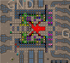
Is it ok If we follow Eval board or Do we need to Consider anything extra for the Best performance?
Kindly Confirm the regarding the same

Regards 
Pavan 

  • Pavan,

    Ideally, to avoid interference between different sections(analog, digital, PLL, clk...) of the device, the GND for each section should be separated.  However, we have been using the same layout for AFE7769 and AFE7769D and haven't had any layout related issues, so it is okay for you guys to follow the AFE7769D layout.  

    One additional point on this, separate digital and analog ground do not mean that the grounds are electrically separate in the system.  To ensure the voltage potential is consistent between all the different power rails, they have to be common at some point, preferably a single, low impedance point.

    Kevin

  • Hi Kevin,
    Thanks for your confirmation.

    Regards 
    Pavan