This thread has been locked.

If you have a related question, please click the "Ask a related question" button in the top right corner. The newly created question will be automatically linked to this question.

DAC38RF89: Minimum SYSREF+/- and DAC_CLK+/- Input Differential Voltage and Min/Max input common mode voltage?

Part Number: DAC38RF89

Hi,

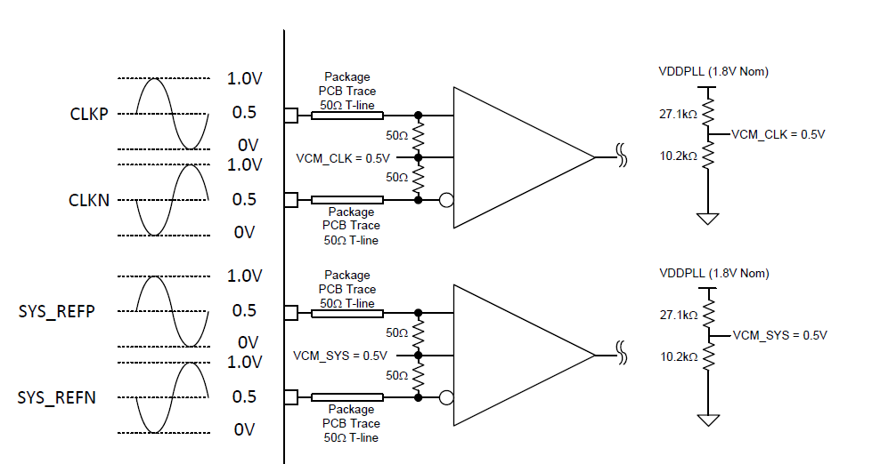
I would like to confirm the minimum required differential input voltage for the DAC38RF89 SYSREF and DACCLK inputs. The datasheet says typical 800mV and max 2000mV. I understand max is top value above which input differential voltage should not exceed, but what is the minimum required input differential voltage for these inputs to guarantee the DAC38RF89 sees valid input switching transitions?

Also, the common mode voltage is listed as 0.5V typical. What is the min/max Common Mode voltage the CLOCK/SYSREF driving circuit must meet? For the clock can AC couple, but SYSREF cannot be directly AC coupled as it has significant DC content. 

Thanks!

  • Hi,

    Please see the link below for your questions regarding clocks and sysref.

    the minimum recommend clock/sysref level is LVDS driver of 400mV. However, we do not recommend driving with this level as it impacts SNR of the DAC. 

    There are internal biases to the clock/sysref driver that may compensate the external bias network, to a limit.

    -Kang

  • Thanks Kang!

    Thanks for providing that info.

    For the swing, I see this in section 6 of the PDF you provided: 

    "Each input leg of the receiver has on-chip 50-Ω termination that is tied to the respective VCM node. Based on the DAC3xJ8x datasheet, the minimum swing for each leg is 400 mVpp of |Vid|. Since the input presented at each pin cannot swing below ground, the maximum swing for each leg can theoretically be 1Vpp of |Vid|."

    Perhaps my terminology is off here, but this is not quite adding up to me. The datasheet specifies 2000mV max peak to peak differential swing, which implies to me the P leg and the N leg can swing up to 2000mV relative to one another. However if this were the case at VCM of 0.5V, then they would drop below ground (0V)  (they would range from -0.5V to 1.5V with 2000mV swing centered at 0.5V CM). How should this max 2000mV swing be interpreted relative to the attached document's note that input at each pin should not swing below ground, effectively limiting to 1V pk-pk at 0.5V common mode? Is this just a restatement of the absolute max voltage specs on the pins (-0.5V low and 1.5V high respectively assuming 2000mV swing at 0.5V common mode)?

    For the minimum swing, from what I have seen typical LVDS drivers would not be guaranteed to meet 400mV VOD. Their output differential voltage (VOD) might range from 250mV or so to 450mV or so. Would it be correct to say that 400mV pk-pk differential input is absolute minimum required constraint such that any driver that cannot guarantee at least 400mV differential from p to n over all range of conditions would not be appropriate to use?

    --EDITED

  • Hello,

    The diagram below can help you understand the swing. The 2000mV is the peak to peak differential swing. LVDS swing can be used as a functional usage, and cannot be used for performance testing.