


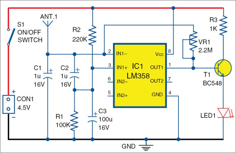
CAN SOMEONE EXPLAIN HOW THIS CIRCUIT WORKS AND WHAT EQUATIONS WHERE USED TO CALCULATE THE VALUES OF RESISTORS AND CAPACITORS.
CAN SOMEONE EXPLAIN HOW THIS CIRCUIT WORKS AND WHAT EQUATIONS WHERE USED TO CALCULATE THE VALUES OF RESISTORS AND CAPACITORS.

