This thread has been locked.

If you have a related question, please click the "Ask a related question" button in the top right corner. The newly created question will be automatically linked to this question.

TDC1000: Ackerberg-Mossberg filter design

Part Number: TDC1000
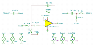
Other Parts Discussed in Thread: LMV881, OPA353, OPA357, , OPA322, OPA4322, REF2912

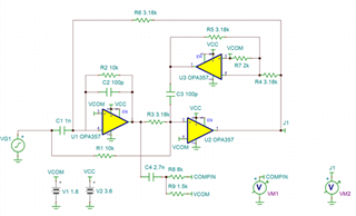
Hello. I am testing the Ackerberg-Mossberg bandpass filter and have questions. The filter enters the generation mode and it worries me a lot. Generation appears both on the PCB and in the TINA simulation. Please tell me what I'm doing wrong?

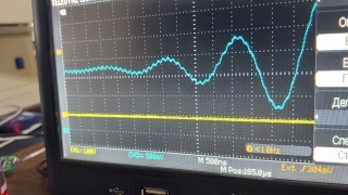
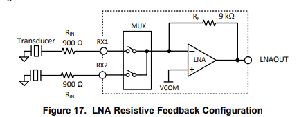
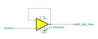
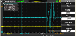
The filter frequency is 500 kHz, the generation appears at the U2 stage.

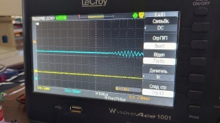
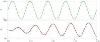
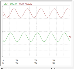
Here is the oscillogram when starting the simulation, at first glance everything is fine

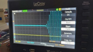
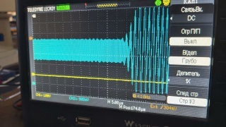
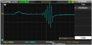
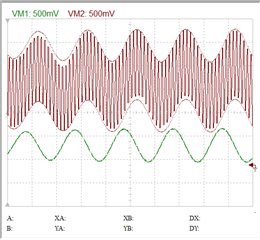
but as soon as I change the frequency, generation appears

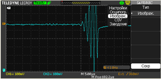
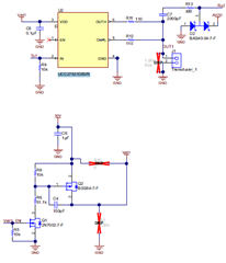
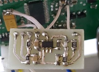
There is also generation on the assembled printed circuit board, but there it is from the very beginning, and does not depend on the frequency change.

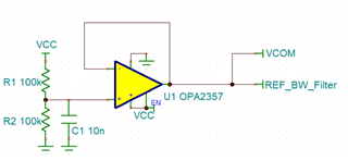
I am using LMV881 operational amplifiers

  • Here is the input

    Here is the output signal

    Here is the output signal magnified, the generation is visible

    Output U2, from which the generation occurs

  • Hello,


    It looks like you are using the SNAA287 application report for the filter design. The AC TINA response looks like the passband is in the 500kHz range. Note, I was unable to find a TINA model for the LMV881 as suggested in the application note. I see your simulation is using the OPA357 in its place. I decided to substitute the OPA353 as the 44MHz GBW is closer to the typical GBW of the LMV881(23MHz) than the OPA357(100MHz).

    Below are my TINA simulations for a 500kHz sine wave. You can see a small fluctuation in the output from a high frequency source. It may be possible that the filter is approaching instability, causing the generation you are seeing.

    What is the input (voltage and frequency) used with your LMV881 operation amplifiers in the real-world tests?

    Here is my TINA file that I am using. Only difference is the OPA353 instead of OPA357:Aleksandr Simulations.TSC

    Finally, what is the reason for the Åckerberg-Mossberg Filter? Have you determined the TDC1000 cannot supply enough gain for the application you intend to implement? 

    Thank you,

    Jacob

  • Thanks for your reply !

    I always have generation on the U2 on the printed circuit board, I just can't get rid of the generation. Maybe I'm doing something wrong in the filter calculation? I didn't want to use this filter as there are a lot of components with the filter and it is difficult to do optimal routing for it. The option without a filter works fine for me, but since I use TDC1000 to develop a gas meter, I have a problem when working in gas. Everything is fine with air, but in gas the signal significantly decreases, and it is necessary to detect the second wave instead of the first. Because of this problem, I am getting more than 2 percent error. If the problem was only in the transition of the wave to the second, I would solve this question programmatically, but it happens that the signal level is obtained at the limit between the first and second waves, and at the same time I often get a false time difference. If you have any recommendations on how to solve this problem, I will be very grateful to you. I am also considering the option of adding one amplification stage without the Ackkemberg-Mosberg filter, since I do not need the notch frequency of the signal absorption. I can make a bandpass filter on one operational amplifier, but I don’t know where it is better to install it, between the LNA cascade and PGAIN or between PGAOUT and COMPIN.

    The waveform in the air without the Ackerberg-Mossberg filter I get like this

    The waveform in natural gas without the Ackerberg-Mossberg filter I get like this

    If there is a solution for this issue without using the Ackerberg-Mosberg filter, this would be the best option.

  • Hello,

    Thank you for sharing the waveforms, I agree the Ackkemberg-Mosberg filter is likely unnecessary. In this case, I would recommend the addition of an external amplifier/filter to the system. So long as the external amplifier is relatively low noise, either position in the signal chain should be about the same for performance. Assuming the gain is equally distributed between the amplifiers, it is typically best to position the least noisy amplifier first. 

    Is the PGA in the TDC1000 currently set to its maximum gain setting of 21dB? If not, it may be possible to realize more gain by altering the device settings.

    Thank you,

    Jacob

  • Is the PGA in the TDC1000 currently set to its maximum gain setting of 21dB

    Yes, gain setting of 21dB

    1) I want to keep the PGA working so that I can programmatically control the gain. Do you think I can install an active filter instead of a passive one, which is indicated in the Datasheet TDC1000? I have created a bandpass filter with an operating frequency of 500 khz, and I want to connect it between PGAOUT and COMPIN. Am I doing the right thing? Or is it better to install it between the LNA outlet and the PGA inlet ?? I saved the matching circuit between the bandpass filters and the input of the comparator, but I doubt the input part whether it is necessary to put a series capacitor C3? I decided to use the OPA322 operational amplifier, since it has a comfortable body and has a pin for sleeping. In the TINA project, I used OPA4322, since I did not find OPA322 in the list, but since the datasheet for them is the same, I think i can use it for modeling.

    The bandwidth of the OPA322 is 20 MHz, can I use a gain of up to 10, with an operating frequency of 500 kHz? Accordingly, I will reduce the PGA gain, and I will get the optimal signal level.

    2)I have another question about the LNA operating mode. The datasheet states that when using low frequency transducers, resistive feedback must be used. When using resistive feedback, high-frequency noise appears at the output of the LNA (several MHz), for this reason I use capacitive feedback. Is this normal? Is it acceptable to use capacitive feedback for 500 khz transducers?

  • Hello,

    Yes, you can install an active filter in the TDC1000. Between PGAOUT and COMPIN works well for filter placement. C3 may not be necessary so long as the amplifier operates in a linear range. OPA4322 and OPA322 will have the same model for TINA.

    As for the LNA, the capacitive feedback mode is set with an internal high pass corner frequency of 590kHz. Therefore, it is usually recommended to use the resistive feedback mode. It may be possible to use the capacitive feedback mode, but you will attenuate the signal of interest.

    One way to reduce the high frequency noise in resistive feedback mode is to change the Rin value to be lower in value. This will in turn increase the gain of the LNA while also reducing the effective bandwidth of the amplifier.

    If the high frequency noise is still dominating the signal, you can use capacitive feedback mode with the active filter.


    Thank you,

    Jacob

  • The problem is that I cannot use this connection, due to the lack of a series capacitor at the input of Rx1 and Rx2. If I put only a resistor between the sensor and the inputs Rx1 and Rx2, I lose the signal, since given that the power supply of the TDC1000 is unipolar, the TDC1000 sends a pulse to the Rx pin before measuring to match the levels (charges the capacitor to VCOM). When using resistors without a capacitor, the Rx pin charges the transducer itself, which negatively affects its parameters. Therefore, at the input I have a RC chain with a nominal value of 300 ohms and 2n, while the 2n capacitor is charged to the VСOM level. Your evolutionary board TDC1000-GASEVM does the same thing, I took the input circuit according to your example. For this reason, I am unable to implement a full-fledged resistive feedback.

    As a Tx driver, I use UCC27531DBVR, and during level matching to VCOM, power is present on it, which guarantees bypassing the transducer at the time of charging the capacitor C7, then I turn off the power, and the UCC27531DBVR output is set to the Z state, which makes it possible to transmit the received echo wave.
    This input circuit turns out to be something between resistive and capacitive, both settings of the TDC1000 give almost the same signal level, except for interference when choosing a capacitive feedback.
    If I'm doing something wrong, please tell me the right way. Examples in a datasheet with resistive feedback without a series capacitor, in practice, is not workable. Plus, if you charge the transducer itself, fluctuations can appear on it, which are difficult to get rid of.

  • Hello again,

    Thank you for detailing the Rx input connections. In that case, I think the best option is in using the active filter and capacitive feedback option. The capacitive feedback should also help with any high frequency noise in the receive path.

    I have never implemented a UCC27531DBVR with the TDC1000 before, but this makes sense as a Tx driver.

    If possible, I would give the active filter a quick try on the PCB to verify everything works as expected.

    Please let me know If you have any questions,

    Thank you,

    Jacob

  • I am now assembling an active filter on a breadboard made by hand, as it will be ready, I will connect it by surface mounting between PGA and COMPIN. It will take me a few days for this, since the OPA322 is out of stock, I temporarily ordered the OPA357 and am waiting for it to be shipped. As soon as I receive the details, I will make the installation of the circuit, I will definitely write to you. Thanks a lot for your advice.

  • Happy to help, 

    I will keep this thread open to verify the active filter works as expected.

    Please let me know how the results look once you finish testing.

    Thank you,

    Jacob

  • Hello. Finally I got the components, now I can test the work of the active bandpass filter. I assembled the circuit by hand, and it turned out to be a small board with outputs of VCC, GND, VCOM, PGAOUT and COMPIN. Dismantled all the components of the passive bandpass filter and soldered my active bandpass filter board.

    But unfortunately at this stage I did not receive a good signal shape, since when the VCOM pin was connected to my printed circuit board, the signal on the PGAOUT pin deteriorated significantly.

    I drew attention to the fact that when using the VCOM output as a reference voltage for my active band-pass filter, an interference appears on the VCOM pin itself, which removes the entire analog section of the TDC1000 from the normal operating mode.

    Next, I decided to add an operational amplifier component as a signal follower, it is an amplifier with a gain of 1.

    At the same time, the waveform has improved, I got a normal waveform at the output of the bandpass filter when it is not connected to the COMPIN pin. When the output is connected to COMPIN, noise appears again, although it is less than in the first variant.

    Next, I decided to use an external voltage reference consisting of an operational amplifier, the input of which consists of a voltage divider.

    At the same time, I received a good signal, although there is still work to be done.

    I received this signal with PGA Gain 6 dB in air, in gas I set 12 dB to get the same signal.

    This is a hand-built prototype, now I have to optimize the circuit. I want you to advise me on a component that I can use as a voltage reference. If an inexpensive solution is available, it is advisable to use a dedicated voltage reference with a power save pin. I can also use an op amp as a voltage reference, but I see no point in using an expensive component since there is no high frequency requirement for this component. Also recommend a low cost (low bandwidth) op amp component with a power saving pin.

    Thank you for your support, I will be very grateful if you can advise me on not expensive components to solve this issue.

  • I also want to share with you my thoughts on an example of the implementation of the gas meter of the gassevm debug board.

    I do not like the probe pulse circuit, which is shown as an example in the gasevm debug board.

    Since the C7 and R13 circuit is involved with the probe pulse, an excess current arises that interferes with the operation of the meter.
    1) an unnecessary input signal appears at the input of Rx, which affects the operation of the analog section
    2) the current at the output of the UCC27531DBVR increases very much, since at a frequency of 500 kHz the capacitor C7 has an equivalent resistance of about 160 ohms, together with P13, 460 ohms are obtained, which, with a probe pulse voltage of 30 volts, is about 65 mA of unnecessary current. For this reason, a large voltage drop is obtained at the output of the DC-DC voltage converter, and the device consumes a large current.

    I tried to change the schema, but I haven't found a good solution at the moment. It would be nice if Texas Instruments further developed a specialized chip to implement the matching of the ultrasonic transducer and TDC1000 with the ability to connect a high voltage for the probe pulse, and would have outputs for the Rx. With a probing pulse, it is necessary to disconnect the C7 and P13 circuits.

  • What do you think about using the REF2912 chip as a voltage reference? The only thing that doesn’t suit me about this chip is that it doesn’t have a pin for power saving. We'll have to put a transistor in order to control the power.

  • If I use an external source of reference voltage, it will not be equal to U / 2. Will this be critical for the operation of TDC1000? In addition, I would like to reduce the reference voltage to 1-1.2 volts in order to reduce the influence of transients during levels matching to the VKOM level. What do you think about this?

  • Hello again, 

    Thank you for conducting the tests with the new active filter. You should be able to use a reference voltage other than mid-supply if desired. Of course this means all stages will need to be referenced to the same voltage.  

    Also note, the output waveform will now be closer to the negative supply rail(GND) than before, so ensure the output swing of the amplifier does not run into any issues with the new configuration.

    I believe the stable external reference may improve performance, especially if the active filter was interfering with VCOM in previous tests. 

    Feel free to update this thread when you obtain test results with the new reference.


    Please let me know if you have any questions,

    Thank you,

    Jacob