This thread has been locked.

If you have a related question, please click the "Ask a related question" button in the top right corner. The newly created question will be automatically linked to this question.

TDC1000: Testing of damaged unit

Part Number: TDC1000

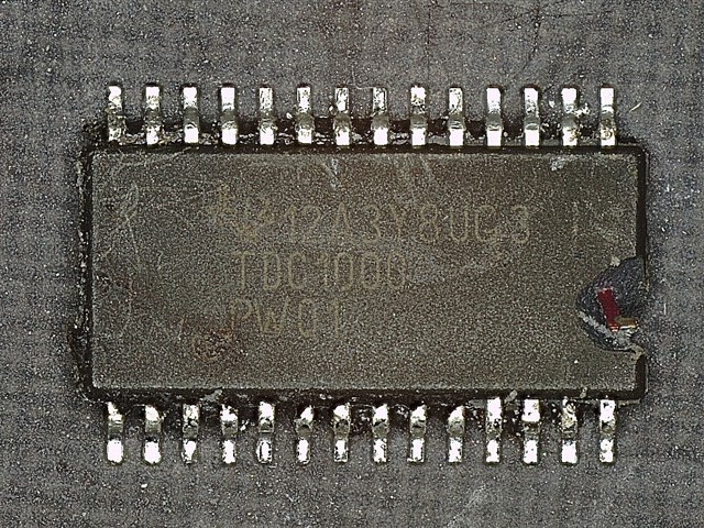
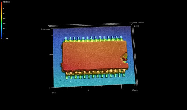
Bosch customer return which was analyzed internally at SSI. FA determined TDC1000QPWRQ1 was the reason for failure but FA was rejected due to the damage to suspect unit. TI Quality advised we submit ticket on here to get in touch with responsible apps and systems experts.

Upper management at SSI Tech and our customer are pushing for some sort of analysis on this component if possible through TI and/or if there is a 3rd party that would take for further testing. Please advise

  • Hello Estrella,

    Thanks for posting to the sensors forum and for bringing up this issue to our attention.

    I am assuming that the visible damage was caused during operation is that correct? I just want to ensure that the device wasn't received in this manner or that the visible damage wasn't incurred during the removal process from the PCB.

    Do you have a count of how many units are showing this damage?

    My thought is that if the damage is only isolated to one unit and this issue is not showing on several units it might be difficult for the team to justify FA. 

    Just to be safe has the SSI team tried placing a new device on the board to ensure the problem does not follow the board?

    A schematic might be useful just to ensure there is no issues with the devices implementation. If you do not want to share in the public forum please send me a private message and you can share via messages directly.

    Best,

    Isaac

  • Hi Isaac,

    It is my understanding that the part obtained visible damage during removal process of the MCU. When the epoxy is flowing over the board, it also flows under this component so removing causes issues as it's basically bonded to the board. This is a warranty claim, so they would like us to try every available avenue to obtain FA of this device. In the past we have returned parts to TI with visible damage but it was determined that the functionality was not affected by this. 

    Preventative action of not removing MCU was proposed to prevent damage during FA, but we were informed that FA is not supported through customer return portal on customer PCBs. This is very understandable, but it causes us to be in a tough position. Are there 3rd party companies which could perform some sort of FA on this with the damage obtained? 

    The failure was noted prior to removal and we did perform A-B-A swap to confirm failure followed the component. Know good boards are used during FA so it was confirmed to not follow board. I am unsure if schematics would be the issue as this device has been used since 

    Our FA tech has some further information he will relay to me tomorrow on how far down the damage goes. He does not believe it goes down to any of the leads or portion of the part that would affect functionality. 

    Estrella

  • Hello Estrella,

    Thanks for the information here, that was helpful.

    If you could please provide more info as to what the actual fail you saw in your system is that might be helpful to me in order to identify what could have been the problem.

    I understand you are trying to pursue every avenue to get FA completed on this device. Let me reach out to the team internally to see if there is anything we can do on our end but for now providing the information from your FA tech will be a good starting point.

    Best,

    Isaac

  • Hello Isaac,

    I have received some feedback from our FA technician which is below. O-scope readings are on the attachment. Thank you for taking time to discuss this, it is much appreciated!

    The damage to the IC is superficial, and the exposed metal is an unused portion of the leadframe that is exposed on the ends of each IC.

    The IC was placed on a known good PCBA and tested. The issue followed the TDC1000. The known good board showed the same increased signal time at the PZT that was shown on the returned PCBA.

    The attached document shows the o-scope readings where the failure follows the TDC1000. Please let me know if you have issues with the document.

    Is there anything else that would be helpful for you?

    -Estrella

    RMA 101361 U2 O-Scope Pics.docx

  • Hello Estrella,

    Thanks for the info and no worries we are always glad to help out!

    I reviewed the scope captures, so it seems like the device still seems to be transmitting the signal used to the drive the piezo transducer, the main difference I noted is that the signal looks rather noisy compared to the good unit.

    Was this added noise also occurring during the listening period of the echo? I am not sure if this added noise would make much of a difference during the transmission period that was shown here but my concern is mainly during the return period. The added noise may falsely trigger the threshold to generate a STOP signal. Is this how the fail was detected or do you monitor the driving signal (signals on the attached doc) as part of the test procedure during production?

    I did check internally with the team and it seems like the FA team cannot accept physically damaged devices because the device typically will indicate various types of failures that usually are not be related to the failure you may have experienced on your system all due to the physically damage on the device. I am waiting to hear back from them to see if there is a 3rd party FA lab that we can recommend to help you perform the necessary checks you need. If you do have more than one device showing this failure though please do your best not to damage the device at removal. You may also want to check with the quality team if you can provide your board if you are concerned about damaging your device at removal and see if they can accept your return in this form.

    Best,

    Isaac

  • Hi Isaac,

    Regarding leaving the device on the board, we have requested this type of FA and it was rejected by TI Quality also.. I have some information from our FA tech that I will list below. It would be great if there are any 3rd part FA labs that can be recommended!

    I reviewed the scope captures, so it seems like the device still seems to be transmitting the signal used to the drive the piezo transducer, the main difference I noted is that the signal looks rather noisy compared to the good unit.

    The main difference noted at two different SSI facilities is the duration of the signal.

    Was this added noise also occurring during the listening period of the echo?

    It is unknown if there is noise during the listening period with the suspect IC.

    In this application, the T0 for concentration is between 30us and 40us. Which is why the known good START pulse is so brief.

    The suspect TDC1000 is still sending the START pulse during the normal listening period where the first 3-4 echoes (STOP pulses) would normally be present. Therefore, the first ~100uS of the listening period is “listening” to the START pulse.

    The TDC1000 is initialized by the microcontroller upon power up. The suspect IC is obviously not interpreting the microcontroller’s commands correctly, as the long signal duration follows the IC, not the PCBA.

    The duration of a good concentration START pulse is less than 4uS. The failing IC’s START pulse duration is ~128uS regardless of concentration or level.

    Correct Concentration Signal Duration

    Failing Concentration Signal Duration

    The duration of a good level START pulse is less than 25uS. The failing IC's initial level duration is ~128uS regardless of concentration or level

    Correct Level Signal Duration

    Failing Level Signal Duration

    Is this how the fail was detected or do you monitor the driving signal (signals on the attached doc) as part of the test procedure during production?

    The sensor failed to read level or concentration in the customer application and was sent back to SSI for Failure Analysis. The o-scope readings show the difference in signal duration, which did not match a known good senor’s signal duration. The signal duration’s excessive length IS why the sensor failed in the customer’s application.

    The sensor passed SSI’s End-of-Line testing. This shows that the sensor was operating normally after production (i.e. the sensor gave valid level and concentration readings)


    -Estrella

  • Hello Estrella,

    Thanks for the detailed information over here. That made the issue being experienced clearer.

    As mentioned by the FA tech the duration of transmission pulses of the bad device are significantly longer than the transmission of the pulses in the good device. I agree with the techs assessment that the device is not interpreting or listening to the microcontrollers commands.

    Since the MCU is used to program the number of transmission pulses emitted by the device. Does the team have a way to check if communication is working properly with the device?

    Best,

    Isaac

  • Hello Isaac,

    I am glad the information helped and have put our FA technicians comments below to your reply.

    The returned PCBA’s failure mode was traced to the suspect TDC1000, as the duration of the START signal was exponentially longer than the signal seen on a known good PCBA.

    The suspect IC was removed, and a known good TDC1000 placed on the returned PCBA. The returned PCBA now has the correct duration of signal.

    A known good PCBA (The same one that donated the TDC1000 for replacement on the returned PCBA) had the suspect TDC1000 placed. The known good PCBA now has the extend duration START pulse.

    Since the extended duration START pulse follows the suspect TDC1000, it rules out the microcontrollers communication as the failure mode.

    -Estrella

  • Hello Estrella,

    I appreciate your reply. My suggestion was not indicating the microcontroller is at fault since the fault seems to clearly follow the device to other boards.

    My question was if the FA engineering team has confirmed the TDC1000's communication pins to be working properly? Since the internal device registers must be used to configure the TX pulses on the TDC1000, this would explain the longer pulses train on transmission. 

    Best,

    Isaac

  • My apologies Isaac.

    The FA technician just gained access to the DEV board and will need some time to get the software installed, and learn it.

    If there is a method of reading the internal registers without mounting the part on the DEV board, that information would be much appreciated.

    -Estrella

  • Hello Estrella,

    The device would just need to be powered and if they could jumper over the communication signals along with ground from the device to the dev board they should be able to confirm if they can talk to the device. After being powered the signals to jumper over would the SCLK, CSB, SDI, SDO.

    Best,

    Isaac

  • Hello Isaac - Please see below from FA tech

    Would the /CSB on the existing TDC1000 on the dev board have to be disconnected?

    I know that the data and clock lines are shared, but sharing Chip Selects can cause some unintended consequences.

    Also, wouldn’t the existing microcontroller need to be disconnected from the suspect TDC1000, so we aren’t fighting two different micro’s trying to communicate at different speeds and times?

    -Estrella

  • Hey Estrella, 

    Isaac is out today but will get back to you on Monday.  I'll try to help in the meantime.  

    Would the /CSB on the existing TDC1000 on the dev board have to be disconnected?

    I know that the data and clock lines are shared, but sharing Chip Selects can cause some unintended consequences.

    Yes, I think it would be best to at least disconnect the existing CSB on the dev board when doing this test.  

    Also, wouldn’t the existing microcontroller need to be disconnected from the suspect TDC1000, so we aren’t fighting two different micro’s trying to communicate at different speeds and times?

    Yes, I agree.  It might be enough to just get the existing microcontroller into a state where it isn't trying to communicate with the chip (maybe manually set the pins to Hi-Z mode), but mechanically disconnecting the communication lines would be best.  

    Another option is to fully remove the existing TDC1000 on the dev board and replace it with the suspect part and see how it works and what the communication signals look like.  Before swapping the parts, I would take some oscilloscope shots of how the original TDC1000 on the dev board look so that you have a fair comparison between devices. 

    Regards,

    Jacob