This thread has been locked.

If you have a related question, please click the "Ask a related question" button in the top right corner. The newly created question will be automatically linked to this question.

PGA900: DEVRAM programming with XDS probe

Part Number: PGA900

Hello,

I would like to ask a few questions regarding the programming of the PGA900, particularly the DEVRAM programming.

I started working on a PGA900EVM a few weeks ago. However, I'm having a hard time understanding how to use the devram to test my code : I accidentally programmed my .hex file I want to test on the OTP two times already, and replacement chips compatible with the EVM's socket are currently hard to find.

I'm using CCS 12.2.0 and a XDS probe to interact with the chip, but I was not able to find clear explanations on how to tell CCS to program my code on the DEVRAM and not on the OTP. What do I have to do to make sure I don't touch the OTP memory when uploading while I'm still testing my code ? Are there example projects made to write only on the devram ?

Best regards,

Benjamin GAY.

  • Hi Benjamin,

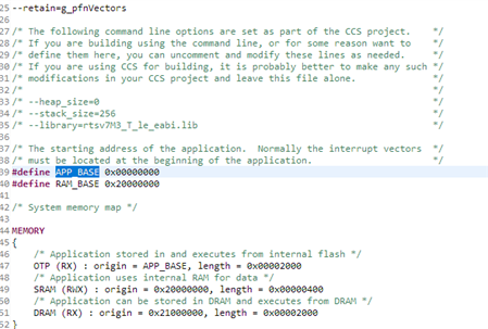
    I can't claim the be an expert here either but I found this snippet of code in pga900.cmd

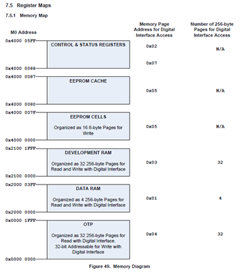
    Correlating with memory map:

    So, I would normally look for a linker file or settings within CCS to define where the application should be stored in memory. For my first pass, I couldn't find these settings so this question might be better for a CCS expert besides a PGA expert. There are some notes and settings in the software quick start guide, I suggest you start there if you haven't taken a look at that yet.

    Alternatively, I wanted to make sure you knew that you can generate a .hex file and then load in the firmware into the GUI or into DEVRAM explicitly. There's instructions in the Software Quick Start guide for generating the .hex file.

    Best,

    -Cole

    As a side note, I'd recommend CCS version is CCS 6.1.1.00022 as shown in the Software User Guide.

  • Hello Mr Macias,

    Thank you for your quick answer. I'll explain in more details what I did :

    I started to work first with the GUI, so I'm aware of its functions. But I have two issues with it. Firstly, I wasn't able to load my .hex file in the devram using the button of the GUI : every time I tried, when I checked the devram afterwards with the read option, it showed me it was blank. Secondly, using the GUI was only a way for me to quickly test the PGA, as I prefer to work on a Ubuntu computer, and the GUI software only works on Windows.

    So I switched on a Linux computer, and started to use the second programming option, with a XDS probe. I looked into the details of CCS to make sure I don't accidentally program on OTP (I found the .cmd file you mentionned, and tried to modify it so all the sections are written either on the SRAM or the DEVRAM), I tried a few times to load the compiled file with the probe, but I got a memory check error. I used the memory browser and found out my second PGA had the OTP memory written (I failed the first one before, with the GUI). But I don't know if the OTP memory got written before or after the switch to Linux + probe.

    I asked this question to make sure I didn't miss something to do in CCS besides the .cmd linker file, as I'm not sure if it's the only file to check in order to program only on devram. That's also why I'm looking for an example project made to program on devram : I want to compare it to my work to be sure of what I'm doing. Do you think I should post those questions on the CCS forum ?

    I also would like to know, what is the purpose of the REMAP register and function of the GUI ? I understand it has something to do with the memory space where the program is loaded, but I don't get its exact role.

    Best regards,

    Benjamin Gay.

  • Hi Benjamin,

    Thanks for the context, everything makes sense now.

    I think you should ask some of these questions to the code composer forum. Specifically, if you focus on the linker and how and why a memory is written to at a high level, then I think you will get the help you're looking for. If the  questions are very PGA focused they'll come back to me. I definitely suggest you have use the orange "Ask a related question" so they have some context. For example, I don't know what memory check error, that sounds like a CCS question to me.

    I also would like to know, what is the purpose of the REMAP register and function of the GUI ? I understand it has something to do with the memory space where the program is loaded, but I don't get its exact role.

    This is interesting! If I understand this correctly, this is a way to ensure you're writing to Dev RAM if we can't quite figure out how to remap the OTP. Essentially, REMAP is used as a quick and easy way to do a quick fix to load a program into Dev RAM if a user was originally writing to OTP. To be a little more direct, when REMAP is set to 1b, the address range of Dev RAM and OTP are swapped. 

    Might be useful if you can set this bit to 1b after establishing communication in init or something like that. 

    That's also why I'm looking for an example project made to program on devram

    Unfortunately, I don't have any example projects that do that. I couldn't find anything in the example project that might help you with this.

    Best,

    -Cole

  • Hi Ben,

    Just closing this thread since we have the other one.

    Best,

    -Cole