Hi,
Working on a design for a OoP sensor on a 4-layer PCB like in this thread: https://e2e.ti.com/support/sensors-group/sensors/f/sensors-forum/1240016/fdc1004-sensor-design-on-4-layer-pcb-submerged-in-liquid?tisearch=e2e-sitesearch&keymatch=FDC1004#
The sensor is about 500 mm long.
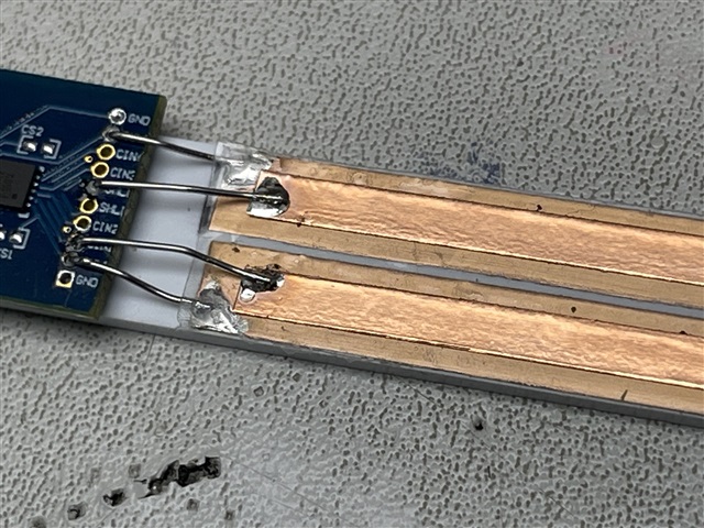
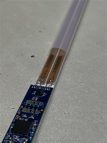
Using a Cu-foil tape mockup on a polystyren core (images below) I get quite high capacitance in air (about 5pF).
If submerged in water the FDC1004 overflows at about 50 mm depth. If putting a thin PTFE-tube around the sensor I get about 9pF at max level, I guess it is ok with the resolution the FDC1004 has but is there some way to optimize the sensitivity when designing capacitive sensors? I have read the guidelines but would like to know more, a simulation software would be nice


I would like to use PTFE heat shrink tubing around the final sensor (4-layer Tg170 PCB) if the PCB can handle the temperature for shrinking the tube , but then there will be no air gap between sensor and the liquid (like in the image above) and I guess the sensitivity will be to high. I could go with narrower electrodes and greater spacing between them but I guess it would reduce the sensitivity as well. It would be nice to have a simulation software to experiment with before I send the design to production.
Finally a question about the OoP design,
Looking at the OoP reference design, the shields are a little bit bigger than the electrodes:

And the CHLD2 is used both as shield and sensor electrode, isn't the larger shield interfering with the sensor (same potential as the sensor electrode)? Should/can I design the sensor with the same width for the sensor electrodes and the shields?
Best regards, L Kull

