This thread has been locked.

If you have a related question, please click the "Ask a related question" button in the top right corner. The newly created question will be automatically linked to this question.

DRV5011: Why VIA is needed in DRV5011ADDMRR

Part Number: DRV5011

Hi,

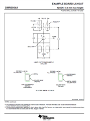
According to the recommended pattern shape in the data sheet, it is recommended to insert the VIA in the middle depending on the application, but in what cases is the VIA necessary? Also, is the purpose heat dissipation? Or escape of excess solder? I would like to confirm whether it is necessary for through holes or whether non-through holes are acceptable. A related question has similar content, but I'd like to confirm it as it doesn't have a definite answer.

Thanks,

Conor

  • Hello Conor,


    I need to check with our packaging team to see if they have any further comment on this. However, I think our packages are developed with the intent of being modular and potentially used across multiple devices from different product lines. The pin configuration and functions section of the datasheet does indicate that the center pad is a thermal pad. While the DRV5011 is not a particularly high current dissipating part, the X2SON package is significantly smaller than the DBZ or LPG package options and has less mass and surface area for dissipating the heat. This via may not be absolutely necessary for lower ambient temperatures; however, when operating towards the max ambient temperature, I would strongly recommend using that via.