DRV5032: If the stability of VCC is poor, the signal will be output at unexpected timing.

Part Number: DRV5032
Other Parts Discussed in Thread: DRV5033

Hi,

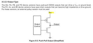
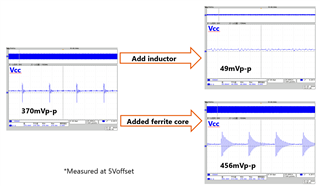
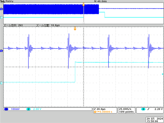
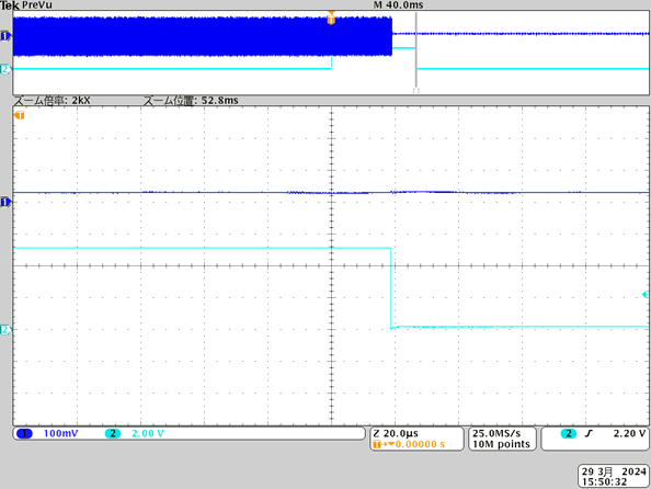
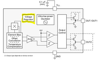
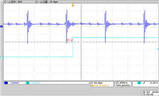
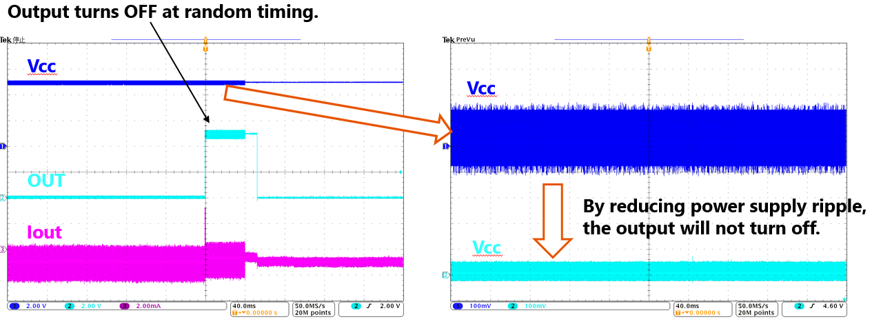
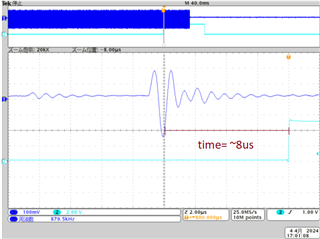
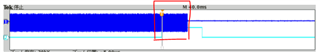
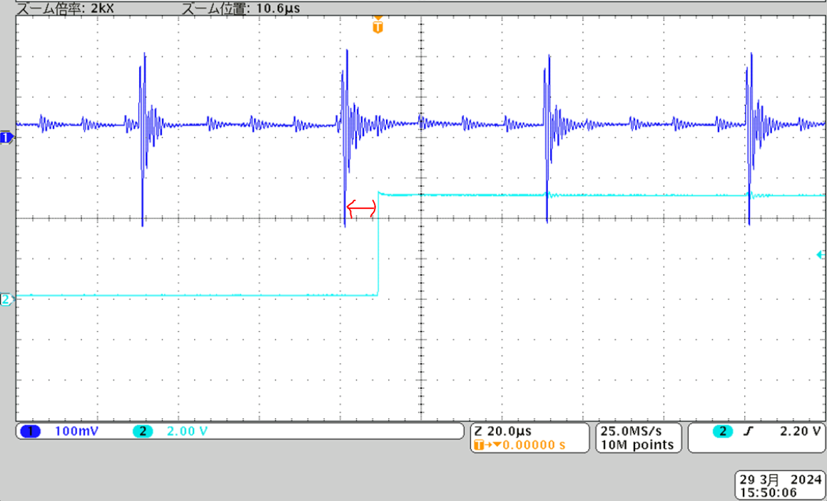
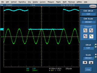
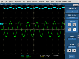
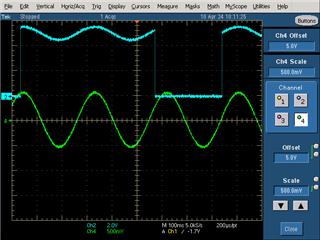
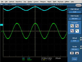
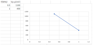
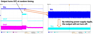
I'm having a problem with DRV5032FA. Even though the positions of the magnet and Hall IC have not been changed, a signal indicating that the magnet is not detected is output at random times, and then a normal signal (magnet detected) is output. When reduce the ripple on the DRV5032FA's power pins, this problem will no longer occur. Could you please confirm the cause of this problem ?

I also investigated E2E and found the following thread.

https://e2e.ti.com/support/sensors-group/sensors/f/sensors-forum/812912/drv5033-output-voltage-falls-for-a-moment/3047348?tisearch=e2e-sitesearch&keymatch=DRV5032%2525252520Vcc#3047348

It is stated in the thread that this is a problem with DRV5033 and does not occur with DRV5032. However, the same problem is occurring with DRV5032FA, so could you please give me some comments?

Thanks,

Conor

  • Hello Conor,

    Thanks for posting to the sensors forum! We have not observed this issue in the past with DRV5032, does the customer provide a decoupling cap on the VCC pin of the DRV5032 as recommended on the datasheet?

    Has the customer attempted to run this test with a clean supply to see if they observe the same behavior? I would like to ensure that the source of the signal switching is not due to a magnetic field change but is indeed the power supply noise that is the source of the problem.

    Best,

    Isaac

  • Hi Isaac.

    Peripheral components recommended in the datasheet are placed. Also, as you can see in the waveform, reducing the ripple on the power pins, regardless of changes in the magnetic field, eliminates this problem.

    Thanks,
    Conor

  • Hello Conor,

    Thanks for confirming that for us! Has the customer tried increasing the capacitance of the bypass cap at the Vcc pin? Increasing this value should help the customer reduce the ripple on their supply before it reaches the device and eliminate the problem. Please also have them ensure that the bypass cap is as close to the device as they can. Having this cap far away from the device reduces its effectiveness at reducing the ripple.

    Like I mentioned there haven't been other reported problems with the power supply ripple causing issues on the DRV5032 in the past so if the customer has done an analysis on how much noise is affecting their device output I can try to see if its possible to replicate this or check with the design team to see if they have any input on this.

    Best,

    Isaac

  • Hi Isaac,

    I understand the measures to reduce VCC ripple. Lastly, I'd like some comments on the operating mechanism.

    The output type of DRV5032FA is Push-pull. Since VCC is used on the high side of push-pull, it seems that VCC noise is somehow affected. Could you please comment on the mechanism behind the malfunction that causes unexpected output due to VCC ripple?

    Thanks,

    Conor

  • Hello Conor,

    We would need a better scope shot than what was provided in order to help identify what the issue it might be causing internally could be.

    If its possible for the customer to collect a really zoomed in scope shot of the Vcc when the device output drops low during a "misdetection" event this would be very helpful. For this capture please ensure that the Vcc is being measured at the device pin so that we can ensure that we are capturing what the device is receiving. The main purpose of the measurement is to ensure that we are capturing the level of the ripple and the timing of the ripple as well.

    Please note that the customer may have to use the tip and barrel method of probing to ensure that they are able to collect an accurate reading for the ripple on the Vcc pin.

    Best,

    Isaac

  • Hi Isaac,

    The layout/capacitors recommended in the datasheet are used, and the usage is within the recommended operating conditions.

    Problem can also be resolved by installing an inductor/ferrite core in the Hall IC's power harness. Adding a ferrite core will increase the ripple voltage as shown in the waveform below, but the Problem will be resolved. What is the reason for this?

    We will send you the enlarged VCC and output waveforms you requested as soon as they are available.

    We will also send you the layout information just in case.

    Thanks,

    Conor

  • Hey Connor,

    Isaac is out of office today and will be back tomorrow. I will look through the thread and see if I can provide additional comments, but just wanted to give you a heads up that there may be a delay in response. Thanks!

    Best regards,

    Jesse

  • Hi Isaac and Jesse,

    Thank you for your reply.
    We'd love to hear your feedback from Isaac. I would appreciate it if you could answer my questions by March 28th.

    Thanks,

    Conor

  • Hello Conor,

    As mentioned, this is likely related to the timing (length of the ripple) as well as the level. Adding the ferrite core increases the level of the ripple but it will also changed the timing/frequency behavior which might explain why the problem goes away regardless of the increased level. Without the zoomed in scope captures I don't have some of the details my design team is asking for in order to look into this further. If we could obtain those captures that would be extremely helpful in trying to obtain an answer for your questions above.

    Best,

    Isaac

  • Hi Isaac

    Sends enlarged waveform information.
    Please let me know if you need any additional information for the investigation.

    VCC_VOUT_waveform.pdf

    Thanks,

    Conor

  • Hello Conor,

    Thanks for sharing the waveforms. Unfortunately, the Vcc signal is not enlarged enough to really see the ripple is it possible to change the enlarge the signal more to see the ripple clearly during the failing condition. For example 100mV/div instead of 1V/div.

    Best,

    Isaac

  • Hi Isaac,

    I send enlarged waveform information. Also, the magnetic flux applied to the Hall IC is 29mT.

    Please let me know if you need any additional information for the investigation.

    Thanks,

    Conor

  • Hi Isaac,

    The Voltage Regulator is mentioned in the functional block diagram of the datasheet. I think this LDO is used to supply the logic inside the IC.
    Is it possible that depending on the PSRR specs of this LDO, the high frequency noise is not cut and is affecting affect the operation of the logic circuit inside the IC?


    When an inductor or ferrite is inserted, the problem is improved even though the ripple is large. We hypothesize that this phenomenon is due to the LC filter consisting of an inductor component such as a ferrite or inductor (10μH) and a capacitor, which cuts high frequency noise. As additional information, the magnetic flux applied to the Hall IC is 29mT. Is it possible for you to comment on the following based on the above content?

    ・Cause of this problem
    ・Reason why malfunctions are suppressed regardless of ripple size
    ・Which conditions in our usage are problematic and possible countermeasures?

    We need to resolve this issue as soon as possible, so we would greatly appreciate it if you could respond as soon as possible.

    Thanks,

    Conor

  • Hello Conor,

    Thanks for the captures and for your patience. We were out on holiday on Friday. Please allow me to review the images provided and I will get back to you.

    Best,

    Isaac

  • Hello Conor,

    Thanks for the scope captures. I think the capture is still not sufficiently zoomed in to determine the length of ripple. Could you try changing time scale to something smaller. You should be able to trigger on the pulse of the DRV5032 with a much smaller time scale, I am mainly interested in just seeing the ripple right before the device fails.

    Two questions on my end:

    On the capture is that the ground reference does not look quite right in the capture, essentially your signal level looks like its 50mV above ground. Can you explain why the signal looks as mentioned?

    Is this issue seen on multiple devices or just one device? Do you have a picture of the the device package to look at the markings and trace codes on the device?

    As mentioned I need to do further investigation before providing a response. I appreciate your patience and understand there is urgency to get this issue resolved. I will work with my team to get your questions answered as soon as possible.

    Best,

    Isaac

  • Hi Isaac,

    Thank you for your prompt cooperation.

    Could you try changing time scale to something smaller.
    Is this issue seen on multiple devices or just one device? Do you have a picture of the the device package to look at the markings and trace codes on the device?

    Please check the attached PDF. This issue is occurring on multiple chips, not just one.
    Package Information and Enlarged waveform.pdf

    On the capture is that the ground reference does not look quite right in the capture, essentially your signal level looks like its 50mV above ground. Can you explain why the signal looks as mentioned?

    Now I don't think I can give you a clear answer as to why the GND is floating, but is there anything I need to check in detail?
    I would like to know the background behind your question.

    Thanks,

    Conor

  • Hello Conor,

    Thanks for the information as well as the image and scope capture. I will be reviewing this with a member of my design team tomorrow I will  get back to you to see if I am able to get any feedback on your questions above.

    Some background behind the GND reference question: I wanted to confirm what the reference point is here to correctly translate the value shown on the scope capture to the appropriate voltage. Based on the information I have reference point is centered at 5V, meaning the reference point is offset by 5V, so whatever is measured above or below that reference point is +/-100mV/div. So for example the lowest point shown in the scope image is ~4.78mV

    Best,

    Isaac

  • Hi Isaac,

    I will be reviewing this with a member of my design team tomorrow I will  get back to you to see if I am able to get any feedback on your questions above.

    Thank you for collaborating with the design team.
    We are planning to update our customers tomorrow, so we would appreciate it if you could let us know the results of the discussion.

    Some background behind the GND reference question

    You mentioned VCC. I mistakenly thought that VOUT was referring to the waveform. VCC ripple noise is noise associated with ON/OFF of relays on the application.

    ・Cause of this problem
    ・Reason why malfunctions are suppressed regardless of ripple size
    ・Which conditions in our usage are problematic and possible countermeasures?

    I apologize for repeating this, but I would like to ask you to comment on three points.

    Thanks,

    Conor

  • Hello Conor,

    I met with the design team and we had some additional items they requested if we could check.

    • Monitor GND during incorrect output time to ensure there are not any potential grounding issues here.
    • Monitor timing of device output change after ripple event, is the output change timing consistent after every event. Test would be to collect 15-20 captures of the fault and check if the timing is the same from a consistent point on the ripple to when the output is high on the DRV5032.


    • Frequency of the ripple, when the error occurs and also during ferrite core capture.
    • Another question we had was if the supply is not cleaned up and the ripple is left does the DRV5032 recover after some time? Or does it remain with the output high until the noise is cleaned up?

    So far to address your questions:

    • Cause of this problem:
      • Continuing to investigate to identify root cause.
    • Reason why malfunctions are suppressed regardless of ripple size
      • The team believes the ripple observed should not be an issue due to 5V operation but we will continue looking into this.
    • Which conditions in our usage are problematic and possible countermeasures?
      • Still have not identified source of problem so we have not identified any other specific problematic issues with the device usage.
      • The only recommendation so far would be to decrease ripple observed by the device by increasing bypass cap. Which the customer has tried and confirmed eliminates issue.

    Best,

    Isaac

  • Hi Isaac,

    Thank you for your update.

    Monitor GND during incorrect output time to ensure there are not any potential grounding issues here.

    The reason why the reference voltage is rising from 5V to +50mV is due to the accuracy of the Power IC being used, and is not due to a GND problem.
    (Probe and GND are properly connected.)

    Monitor timing of device output change after ripple event, is the output change timing consistent after every event. Test would be to collect 15-20 captures of the fault and check if the timing is the same from a consistent point on the ripple to when the output is high on the DRV5032.
    Frequency of the ripple, when the error occurs and also during ferrite core capture.

    Pages 1 to 4 of the PDF are waveforms (20 sheets) in case the problem occurs. Page 5 of the PDF shows waveforms (4 sheets) when no problem occurs when inserting ferrite.

    Enlarged waveform when an error occurs and when a ferrite core is inserted.pdf

    Another question we had was if the supply is not cleaned up and the ripple is left does the DRV5032 recover after some time? Or does it remain with the output high until the noise is cleaned up?

    Due to the configuration of the system, it is not possible to continue adding noise to the power line. What we have confirmed so far is that, as shown in the first post, if noise occurs on the power line, the output remains High.

    We would also like to share with you our current hypothesis.
    -This problem occurs regardless of the noise ripple.
    ・This problem does not occur as a result of inserting an LC filter or ferrite.

    From the above two points, it seems that the frequency of the noise, rather than the ripple of the noise, is somehow involved. For example, the internal voltage regulator (LDO) supplies power to the internal logic circuit, but due to the LDO's PSRR characteristics, it cannot cut out high-frequency noise, which may affect the logic circuit in the subsequent stage, causing problems. There are etc.

    Please continue to check the following three points.
    ・Cause of this problem
    ・Reason why malfunctions are suppressed regardless of ripple size
    ・Which conditions in our usage are problematic and possible countermeasures?

    Thank you to the design team and your help.

    Conor

  • Hello Conor,

    Thank you for the reply here are some comments if you could help confirm.

    The reason why the reference voltage is rising from 5V to +50mV is due to the accuracy of the Power IC being used, and is not due to a GND problem.
    (Probe and GND are properly connected.)

    I understand the reason we see a shift in the voltage, and that the probe and GND are properly connected. Some clarification on what I requested is if its possible to probe GND to ensure that our ground is stable during the period when the relays are switching.

    Pages 1 to 4 of the PDF are waveforms (20 sheets) in case the problem occurs. Page 5 of the PDF shows waveforms (4 sheets) when no problem occurs when inserting ferrite.

    Thank you for providing the enlarged captures. Based on all the captures provided it looks like the issue occurs consistently every ~8us after the lowest point in the power supply voltage. But its also very consistent at the point in which the issue occurs. It looks like there is supply is noisy for most of the capture but the issue is always occurs at the same section of the relay switching sequence before the signal cleans up. Is there a difference in the ripple right before the capture occurs vs most of the noisy period? Is the DRV5032 controlling the relays hence why the supply cleans up after the DRV5032 encounters the issue?

    From the above two points, it seems that the frequency of the noise, rather than the ripple of the noise, is somehow involved.

    I am looking into this same point hence why I asked the frequency of the noise in my previous question. It looks like the ripple when it fails is ~1MHz while the ripple with the ferrite is ~500kHz. I will be trying to look at this in the lab to see if I can emulate some ripple.

    I will get back to you once I have more info. Looking forward to any other info you may have. Thanks!

    Best,

    Isaac

  • Hi Isaac,

    Some clarification on what I requested is if its possible to probe GND to ensure that our ground is stable during the period when the relays are switching.

    OK, Customers have already confirmed that GND is stable. Additionally, customer find it time-consuming to acquire waveforms. I would like you to confirm and verify the information I sent to you as much as possible.

    Is there a difference in the ripple right before the capture occurs vs most of the noisy period? Is the DRV5032 controlling the relays hence why the supply cleans up after the DRV5032 encounters the issue?

    Is it possible for you to make a judgment based on the waveform I sent for the reason I stated earlier?
    Noise occurs at a constant period and frequency. This is because the noise is caused by the relay turning on and off. Looking at the waveform, there is no difference in the ripple before and after the malfunction occurs.

    Is the DRV5032 controlling the relays hence why the supply cleans up after the DRV5032 encounters the issue?

    Yes, the customer said, "The system cannot continue to provide noise," so I think your understanding is correct.

    I am looking into this same point hence why I asked the frequency of the noise in my previous question. It looks like the ripple when it fails is ~1MHz while the ripple with the ferrite is ~500kHz. I will be trying to look at this in the lab to see if I can emulate some ripple.

    Thank you for reproducing the results in the lab. There are additional points that I would like to confirm.

    When I checked the waveform, the ripple when the ferrite was inserted was about 500kHz, but the ripple when the malfunction occurred was about 1MHz. The ripple rejection rate (PSRR characteristics) of the regulator that supplies power to the IC's internal circuits (logic) is quite low around 1MHz, and the regulator cannot sufficiently cut out high-frequency noise, which may affect the internal circuits and cause malfunctions. Could this be occurring? I would like to know the PSRR characteristics of the internal regulator. Also, if high-frequency noise passes through, are there any parts of the IC's internal circuitry that may accidentally output a high signal? If it is difficult to send internal information on the E2E forum, we may exchange information via private message or email.

    Thanks,

    Conor

  • Hi Isaac,

    Were there any updates from your discussions with the design team?

    Thanks,

    Conor

  • Hello Conor,

    No updates from my side. My next item is to see if I can replicate the issue the customer is showing at 1MHz ripple.

    The ripple rejection rate (PSRR characteristics) of the regulator that supplies power to the IC's internal circuits (logic) is quite low around 1MHz, and the regulator cannot sufficiently cut out high-frequency noise, which may affect the internal circuits and cause malfunctions. Could this be occurring? I would like to know the PSRR characteristics of the internal regulator. Also, if high-frequency noise passes through, are there any parts of the IC's internal circuitry that may accidentally output a high signal?

    This was my theory as well but I cannot confirm if this is the issue until I have tested this out myself. I can check with the design team once I have results to see if we have a PSRR spec for this device. If you have sensitive information to send please feel free to send me a direct message. Please not this is a public forum so please do not share any sensitive documents.

    I was working on another test so I did not have a chance to set this back up. But I should get a chance to look into this tomorrow.

    Best,

    Isaac

  • Hi Isaac,

    An end customer has requested the results of a survey.
    Sorry to bother you, but is it possible for you to share the results of your investigation?

    Thanks,

    Conor

  • Hey Conor,

    I did some testing on my end and was able to see similar results as your customer. Unfortunately, I am not able to replicate their exact signal so my testing was done by adding sinusoidal ripple to the power supply at 1MHz and 500kHz. During the test I would place and remove a magnet from the sensor to ensure that I could see the device respond to the magnetic field as expected. If the device didn't change the output based on the magnetic field then it was deemed as not functional. For the signals below the Blue signal is the DRV5032 output and the green signal is the Vcc offset by 5V so the sinusoidal voltage swings above and below the 5V mark.

    Running the ripple at 1MHz the device stopped working when the ripple at the supply was ~500mVpp and the output will go into a high state as observed by the customer. When the ripple was reduced on the supply the device would recover as observed by your customer.


    400mVpp @1MHz                                                             500mVpp @1MHz

    When changing the ripple frequency to 500kHz the ripple on the supply necessary to cause the device to fail increased. So, in this instance the device stopped working when the ripple at the supply was ~1200mVpp with the output remaining high as well.


    1100mVpp @500kHz                                                      1200mVpp @500kHz

    Customers questions:

    ・Cause of this problem- The supply ripple level and frequency are too high for the current device configuration on their board.
    ・Reason why malfunctions are suppressed regardless of ripple size- The device susceptibility to the power supply ripple seems to be dependent on the frequency of the ripple. Having lower frequency ripple appears to have a better immunity to the noise on the power supply compared to higher frequency power supply ripple.
    ・Which conditions in our usage are problematic and possible countermeasures?- The power supply noise coupling to the device is too high and needs to be reduced, this can be mitigated by increasing the capacitance on the Vcc bypass cap of the device.

    Let me know if there are other questions!

    Best,

    Isaac 

  • Hi Isaac,

    Thank you for sharing the reproduction test. I have additional questions based on the verification results.

    Q1
    Is it correct to understand that this malfunction is not lot dependent and is a characteristic of DRV5032, since it was reproduced in the lab? I'm wondering if there are variations in malfunction depending on the chip.

    Q2
    Is it correct to understand that the ripple frequency/level has a linear relationship as shown in the graph below?

    Q3
    Why does this malfunction depend on the frequency of the power supply ripple? Also, why does the ripple level cause the IC to malfunction? I'd like some insight into the mechanism behind the malfunction.

    Q4
    When suppressing power supply ripple, are there any recommended limits for ripple frequency/level?

    Thanks,

    Conor

  • Hello Conor,

    Let me help address your questions.

    1. Q1: Is it correct to understand that this malfunction is not lot dependent and is a characteristic of DRV5032, since it was reproduced in the lab?
      1. Correct this is not a malfunction but just a characteristic of the device. Essentially every device would have the same behavior at higher frequencies the point at which it does not react to magnetic fields might differ due to variation.
    2. Is it correct to understand that the ripple frequency/level has a linear relationship as shown in the graph below?
      1. The expected relationship is not expected to be linear but have some curve. It will follow a trend in the direction as shown here but a linear relationship is not expected. 
    3. Why does this malfunction depend on the frequency of the power supply ripple? Also, why does the ripple level cause the IC to malfunction?
      1. There are blocks inside the IC that are sub-regulated from the supply voltage, when the frequency and level of the ripple are too high the internal regulator cannot keep up attempting to regulate the supply voltage due to the excessive ripple.
    4. When suppressing power supply ripple, are there any recommended limits for ripple frequency/level?
      1. I don't have a spec value for this but I can check with the design team to see if there is a guideline for this value.

    Best,

    Isaac

  • Hi Isaac,

    Thank you for your reply.

    There are blocks inside the IC that are sub-regulated from the supply voltage, when the frequency and level of the ripple are too high the internal regulator cannot keep up attempting to regulate the supply voltage due to the excessive ripple.

    I would like to know why the internal LDO loses control when the ripple level/frequency is too large. I initially had the following hypothesis.

    ・Due to the PSRR characteristics of the internal LDO, high frequency noise passes through the internal LDO and has an adverse effect on the internal logic circuit.

    However, from your answer, this malfunction is not only affected by the frequency of the noise, but also by the noise level. I need a detailed view of the malfunction mechanism to confirm the validity of the countermeasures, so would it be possible for you to discuss this with the design team?

    I don't have a spec value for this but I can check with the design team to see if there is a guideline for this value.

    Thank you. I'm waiting for a reply from the design team.

    Thanks,

    Conor

  • Hi Isaac,

    Were there any updates from your discussions with the design team?

    Thanks,

  • Hello Conor,

    However, from your answer, this malfunction is not only affected by the frequency of the noise, but also by the noise level

    Correct, the behavior is caused by both the level and frequency of the ripple. Essentially the lower frequency the ripple is the higher the level that is accepted by the device. For higher frequencies the level is lower, hence why when I provide a 500kHz ripple the level can be much higher than at 1MHz before I see the device stop responding to the field.

    I need a detailed view of the malfunction mechanism to confirm the validity of the countermeasures

    Can you elaborate on what you mean by a detailed view of the malfunction mechanism? I am not sure what you are trying to obtain here.

    Best,

    Isaac

  • Hello Conor,

    Thanks for the patience here. I spoke with the design team and based on the noise it is not recommended to have noise above 100kHz on your power supply. Essentially you theory is correct, at 1MHz the internal LDO is not capable of filtering the noise caused by the relays. Since its not able to filter out the noise it gets directly coupled into the other blocks that are sub-regulated by this internal LDO.

    In my testing that is why the device becomes more susceptible as I increase the frequency. The level only matters because of the filtering capability of the LDO circuitry at a given frequency. For example at 500kHz the filter might only be able to attenuate -3dB vs -10dB at 100kHz. I hope this helps please let me know if anything else is needed, I am not sure what else I may be able to provide to get this issue completely resolved on the customers side.

    Best,

    Isaac

  • Hi Isaac,

    Could you please provide information on acceptable frequencies depending on the noise level? In other words, is there any information on the PSRR characteristics of the internal LDO? The customer is concerned about the above because it is not a linear characteristic in the answer below.
    (We are asking this question with the premise of reducing the noise level.)

    The expected relationship is not expected to be linear but have some curve. It will follow a trend in the direction as shown here but a linear relationship is not expected. 

    Thanks,

    Conor

  • Hello Conor,

    The noise level is mainly relevant because the customer is past the recommended frequency of the internal LDO. The recommendation for the DRV5032 is for the noise at the Vcc input to remain below 100kHz in frequency, since the noise frequency is 10 times past this recommended value the effectiveness of the filter has been reduced significantly.

    The behavior is expected to be linear when looking at the relationship in terms of dB but since the conversion to dB is not linear the behavior in terms of voltage may not be precisely linear but could have a slight curve.

    I think the main goal of the customer should be to reduce the frequency of the noise, since the main reason the sensor output is being affected is due to the the frequency of the noise it makes more sense to go after this problem. This should also be easier for the customer to change, since they can add extra capacitance to their power lines or a filter after the relays to eliminate the high frequency components of the noise. If the noise was operating at the recommended frequency then the level is not high enough for the sensor to have an issue.

    Best,

    Isaac