TMAG3001: Hall element position

Part Number: TMAG3001

Tool/software:

Dear,

We plan to use TMAG3001 component on one off our new design.

 Electronic data are clear for us.

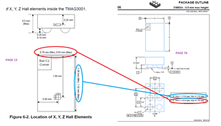
We have question about mechanical position of hall element in the case.

Datasheet indicate 0.25mm from top but 0.25 ± XX ? What are the min and max value ?

Same question for other parameter: position from the side of the case.

Regards,

Aymeric Dunoyer

  • Hello Aymeric,

    Thank you for considering to use Texas Instruments.  I am forwarding your question to our packaging team.  As some of those personnel are in China, I may not have an update for you until Monday.

  • Dear Patrick,

    What are the dimensions of the case of  TMAG3001 ?

    Page 13: 1.28-1.32 x 0.79-0.83 mm

    Page 70: 1.256-1.316 x 0.764-0824 mm

    Witch one is correct ?

    What are the position of X and Y relative to Z (center) hall elements ?

    Regards,

    Aymeric Dunoyer

  • Hi Aymeric, 

    Apologies for the delayed response, we are still talking to our packaging team regarding your question about the package's outer tolerances. However, I have some new information regarding the hall element placement relative to the device's pads.

    Below is a top-view image of the package with the hall elements circled in green. Since this is a DSBGA package, the midpoint between the centers of balls B1 and B2 is the die center. This will be the new reference point for the hall sensor placement.


    As described in the image, the Z element center is offset 7um on the horizontal axis and 338um on the vertical axis. As for the placement of the X and Y hall elements relative to the Z axis element, please refer to the following diagram:


    The X element is 99.9um away and the Y element is 98.7um from the center of the Z axis. This image is using the same coordinate system as the first image. I'm still working on getting the packaging tolerances clarified, and I'll let you know once I get that information, if you need it. Hopefully with the provided measurements you won't have to calculate the hall element location based on the package's edges.

    Thanks!

  • Hi,

    Thank you for theses informations so we need to considere center of the package instead of the sides.


    Will the datasheet be updated with these elements?

    Regards,

    Aymeric Dunoyer

  • Sorry I hadn't seen your first drawing !
    I did the same.

    Just waiting for tolerances now.


    Regards,
    Aymeric Dunoyer

  • Hi Aymeric, 

    I'm glad I could help. Since the package is die-sized, the ball grid is manufactured to the same tolerance as the silicon, meaning that the expected tolerances of the hall elements' positions relative to the balls are very small (<1um). If you base your placement off of the midpoint between B1 and B2 you should have plenty accuracy given the sensitivity of the device. With regards to the tolerances of the outer edges of the package, I am still waiting on new information from the packaging team. My apologies for the delay.