- Ask a related questionWhat is a related question?A related question is a question created from another question. When the related question is created, it will be automatically linked to the original question.
Original question:

Dear TI:
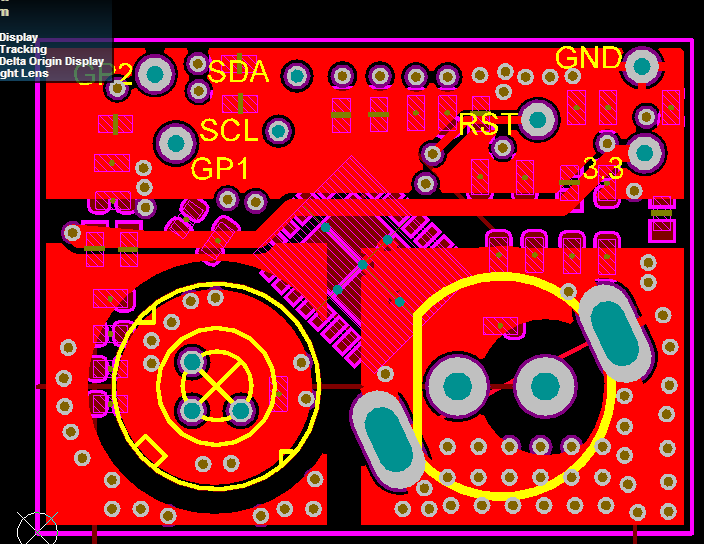
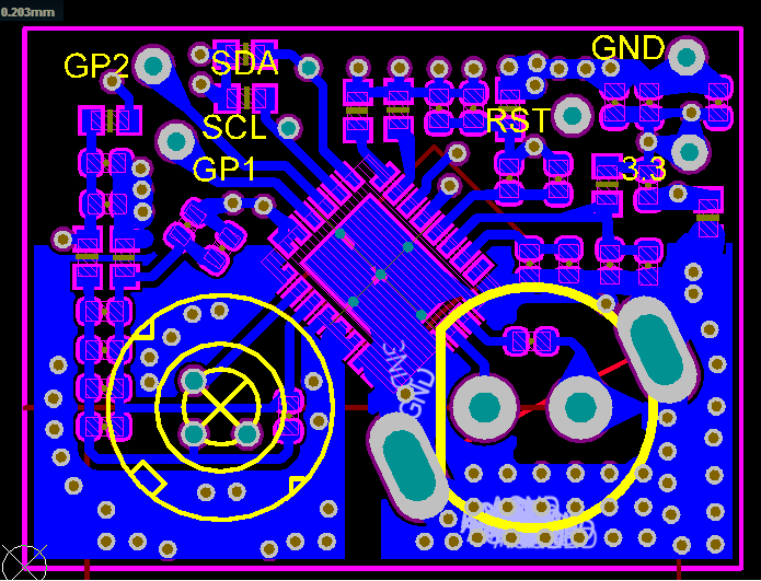
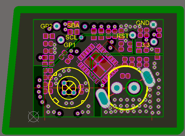
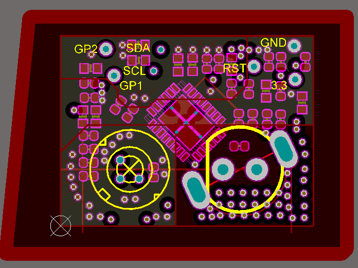
I Design a pcb used opt3101 and found xtalk offset too large compared with EVM board. doc.files
log.doc
readI2C: 88 , addr: 59, data: 18229
readI2C: 88 , addr: 60, data: ffd25a
readI2C: 88 , addr: 59, data: 181e1
readI2C: 88 , addr: 60, data: ffd25a
iphase_xtalk: 18229, qphase_xtalk: ffd25a, iread: 181e1, qread: ffffd25a, mRead: 98785
c0: 16, small: 65536, big: 131072, xtalkScale: 2
(The laser tube is opened to cover the pd receiver tube, and the xtalk is large. )
Test process:1.Turn on the power, 2.Block pd,do measureAndCorrectInternalCrosstalk、measureIllumCrosstalk,3. remove pd obstacle,do measurePhaseOffset with a fixed distance。
The register read and write are all ok.
Can you give me some advise how to address the problem ? thanks