Other Parts Discussed in Thread: IWR1642BOOST
Hi,
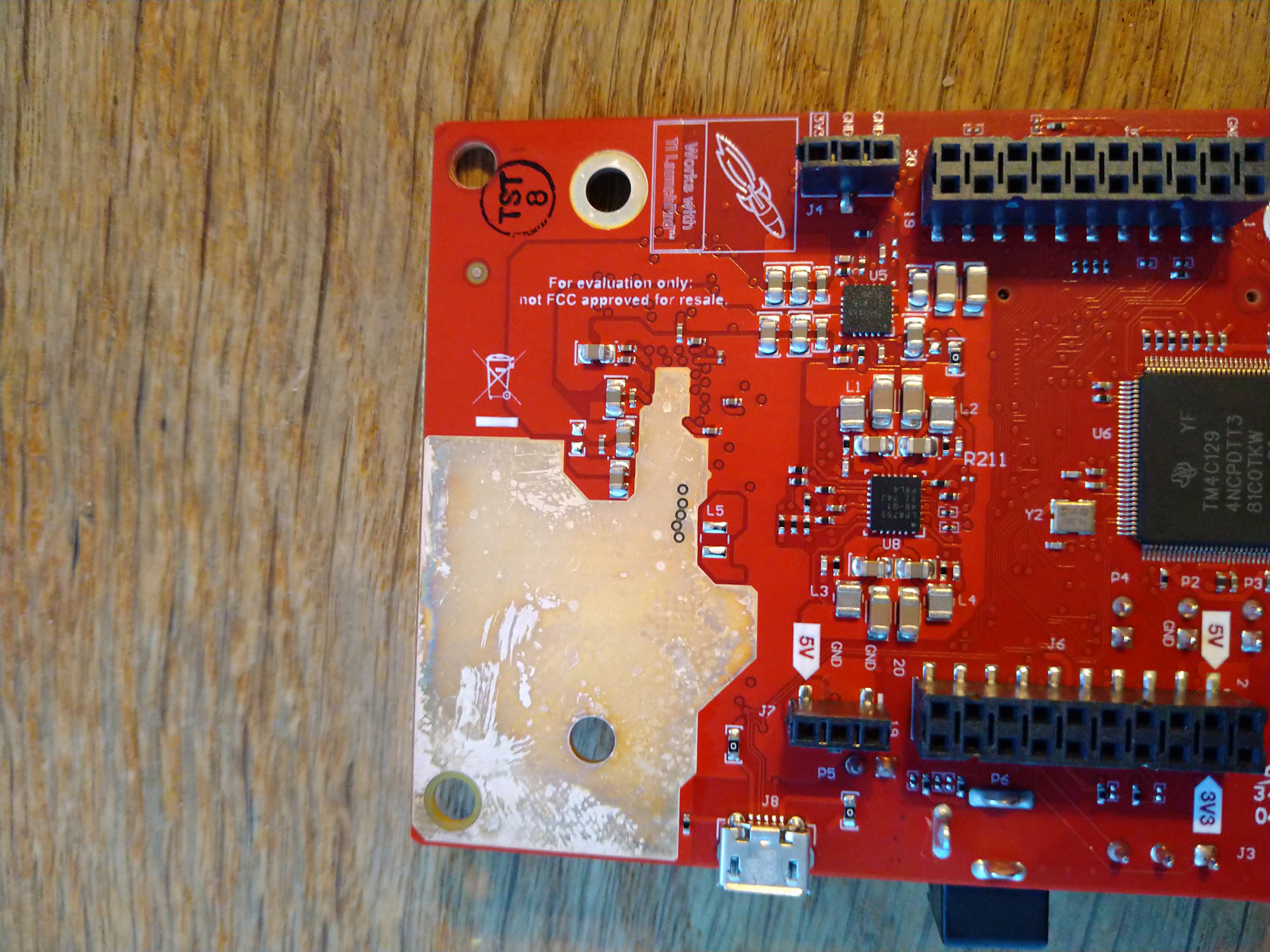
We're in the process of designing a custom PCB for an IWR1843 application, and I have a few questions regarding the antenna design. First of all we're quite cramped on space, and since we don't need any angular information for our particular application, we will have 1 TX and 1 RX antenna. Furthermore, another restriction, is that the PCB will be 30 mm in diameter. So based on that, I'm wondering about the following:
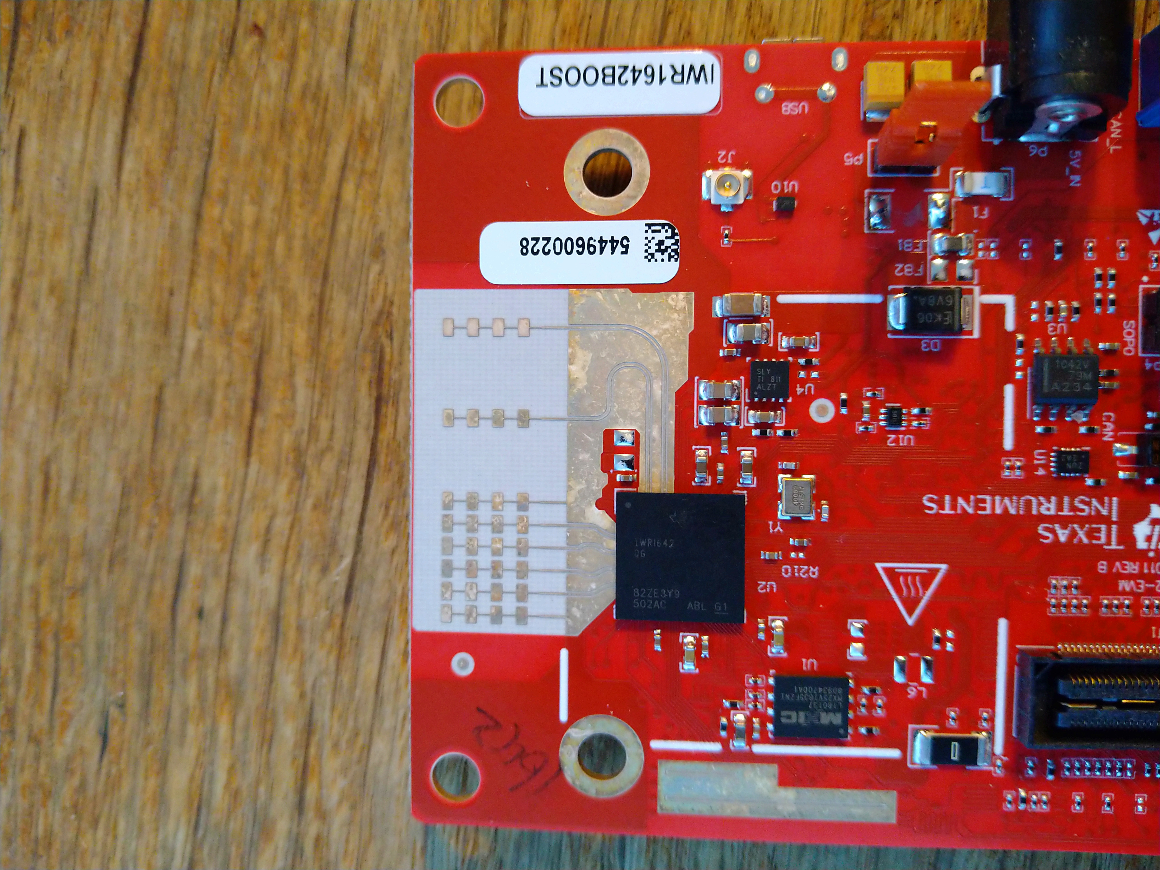
1. On the IWR1843 BOOST eval board, it seems like there are two antenna patch strips on both sides of the RX antennas connected to GND. Why is that, and what is the consequence of not including them?
2. Due to the geometry of our PCB, we were thinking of curving the RX and TX antennas to follow the curvature of the PCB, instead of having them as straight lines. Will this be a problem? Since we're not interested in any angles, and just using one antenna of each, I assume there would be no phase issues. Am I correct?
3. On the evaluation board there is a pretty large GND area exposed under parts of the antennas. Is there a reason why this is exposed and not designed as a layer in the middle parts of the PCB? Is there a consequence if incorporating this as an inner layer, and not exposed? Since we are pretty cramped for space, we would like to use the other side of the PCB for other components.
Thanks!