This thread has been locked.

If you have a related question, please click the "Ask a related question" button in the top right corner. The newly created question will be automatically linked to this question.

TS3V712E: Video signal SW

Part Number: TS3V712E
Other Parts Discussed in Thread: SN74CBT16232, TMUX646, SN74CBT16292

Hi team,

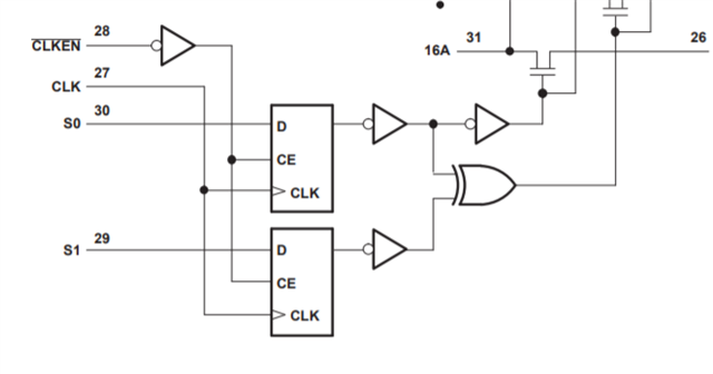
A customer is looking for a device to switch the signal from CPU and FPGA to LCD.

Please see the file for system block diagram.

I am thinking if this device is suited, but he may need to use more than 3 pcs in every system.

Could you suggest  a relatively simple solution?

Best,
Zeming

 LCD System.xlsx

  • Hey Zeming,

    Some more information on this would be useful here. Could you provide information on the voltage range and frequency of the signals we will be multiplexing? If I'm understanding properly only pins 6 through 31 are to be multiplexed here, correct?
    Looks like these will be mainly the Data signals. Are these all differential or single ended. LCD typically has differential I believe but some clarification on this (and what voltage levels will be used) would be helpful for determining the proper device. Additionally the CLK frequency would help in finding the device with enough bandwidth. 
    The indicator I/O's (STBYB, RESETB, DE, etc.) I'm assuming won't be a limiting factor in this but if you could determine the voltage levels on those as well, it may be something to look at. 

    There is a app report (Differential Passive Signal Switch on Computing) with a similar topic. This will be for differential switching however. 

    TS3L500AE may be a good starting point to look at for LVDS switching. It's a 8 channel 2:1 but has some extra 2:1 switches that are purposed for LED's but can be used for some indicator pins if needed. You'll probably need 3 pieces as you mentioned. We may even be able to put all signal on two devices if it's single ended data. Something like 2x SN74CBT16232, which is a 16 channel 2:1.   
    This, of course, is me assuming some of these characteristics just to help get the ball rolling. I wouldn't recommend this as a final solution yet, so if you can provide the information from above though, we can see what the best fit would be.

    Thanks!
    Rami

  • Hi Rami,

    Thank you very much.

    The RGB is single ended. CLK frequency is <10MHz, and all signals are 3.3V Logic High.

    So 2x SN74CBT16232 should be good, I have promoted this solution to the customer.

    Please let me know if any better idea.

    Best,
    Zeming

  • Zeming,

    The 16 channel CBT family will be your best bet for switching on the smallest number of devices possible. 

    3x TMUX646 would be the next best bet in terms of IC count but a better option in terms of functionality. This is a newer device in our portfolio. While there would be an extra device the footprint space would be less since the TMUX646 comes in the nFBGA package (6mm2). While the smallest package the CBT would come in is the TVSOP (50mm2). The TMUX646 would provide better performance and has some extra features (ie powered off protection and 1.2V logic compatibility).

    Thanks,
    Rami  

  • Hi Rami,

    Thank you very much. Your advice really helps a lot!

  • Hi Rami,

    Sorry to open this thread again.

    Actually only 22ch will be used, so 2pcs SN74CBT16232 is over spec.

    Then I suggested SN74CBT16292 6ch SW x 2pcs.

    The customer wants to know why 292 does not have /CLKEN, and how this pin can be leveraged?

    Best,
    Zeming

  • Hi Zeming,

    These devices are not 1:1 devices. They is a difference in architecture for logic and the switches itself. 

    The difference in switch architecture is that the unused ports are pulled down using internal pull down resistors.

    The difference in logic is shown below:

    232:

    292:

    This difference in logic essentially is that the 232 is using logic timing circuits (in this case D flip flops) to synchronize switch state changes with a clock input as well as allowing A to connect to B1 and B2 at the same time. 

    The 292 on the other hand is a simple inverter pathway - and is hardwired to not allow XA to be connected to XB1 and XB2 at the same time. That being said if the ability to switch the switches state with a clock input can be achieved by adding external timing circuits. Basically add a D Flip flop with a clock enable - where the input is your control signal "S" and the Q0 output is hooked up to the "S" input pin of the switch. The output of the flip flop will change to the input level when the clock signal is read (commonly a rising edge application, but could be falling edge) - if the D Flip flop is not enabled it will hold its last state that was clocked in. 

    If you have any other questions please let me know!

    Best,

    Parker Dodson

  • Hi Parker,

    Thank you very much!