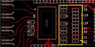
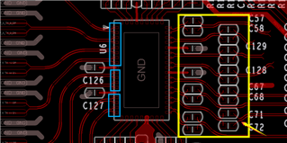
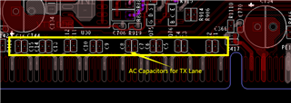
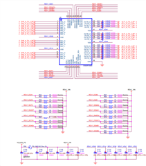
This thread has been locked.

If you have a related question, please click the "Ask a related question" button in the top right corner. The newly created question will be automatically linked to this question.

DS80PCI800 Schematic Check

Other Parts Discussed in Thread: DS80PCI800

我们专案RS-C236E2X3,采用TI DS80PCI800ReDriver方案,客户测试时有发现如下问题:

插Intel 82599的网卡测网络流量一段时间就会出现网卡被重置,无法识别,丢包等各种情况,麻烦检查优化我们线路设计,谢谢!

  • Attached is our DS80PCI100 circuit diagram,Please help check,Thanks

  • Hi King,

    This portion looks good to me. I would recommend that the designers double check that AC coupling capacitors are placed on the input lines (EXP_A_TX_0_DP all the way through EXP_A_TX_7_DN) somewhere in the complete schematic, they are needed for proper I/O functionality at high speeds.

    Best,

    Evan Su

  • Hi Evan,All AC Capacitors are placed close to the chip,The attached figure is the placement of our Layout,In addition, Please check whether  Equalizer & De-Emphasis Settings are appropriate,Thanks

  • Hi King,

    The capacitors look good then. Regarding the equalization and de-emphasis settings, it's hard to predict what settings will work the best just by looking at the schematic, and we recommend finding the best fit through experimentation. It looks like all the settings are currently set to the minimum level (Level 1). Assuming you have a method of adjusting the pin levels within the design, you could start from the minimum settings and increase the equalization and de-emphasis step by step until the results are satisfactory. You could also consult Table 2 and Table 3 in the datasheet, which have suggested equalization and de-emphasis settings for certain trace dimensions, to have an idea of what to expect.

    Best,

    Evan Su

  • Hi Evan,

    Thank you for your suggestion. We'll try it step by step

  • Hi King,

    I reexamined the PCB layout schematic and would like clarify my comment from earlier today: assuming that the chip in the picture is the DS80PCI800, I can see that the AC coupling capacitors on the chip that you boxed in yellow are attached to the OUTB_x and OUTA_x pins, and this is fine. What I suggested that you double check are that the traces for the INB_x and INA_x pins (boxed in blue in the attached image), which are on the left side of the chip, have AC coupling capacitors too at some point along their length. 

    The capacitors do not need to be next to the chip, but they should exist somewhere along EXP_A_TX_0_DP, EXP_A_TX_0_DN, etc. If you already put capacitors at the beginning of these traces for example, then that would be fine.

    Best of luck with your design, let us know if you have more questions in the future. I will mark this thread as "TI thinks resolved" for now.

    Thanks,

    Evan Su

  • Hi Evan,

    Thanks for your detailed inspection. The AC capacitor for TX signal is placed at the end of other PCIe connector.

  • Should be all good then!

    Sincerely,

    Evan Su