


Other Parts Discussed in Thread: CC2650
Hello,
We have designed a PCB with analog switch TS5A3160.
At output of analog switch Display is connected.
It was supposed that we will control the Display power using TS5A3160 switch and turn the display power OFF when not required to save coin cell battery life.
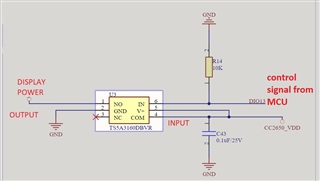
Our schematic is as shown in the Image.
I have written a simple GPIO toggling code in CC2650 microcontroller board
I have verified that
pin no 2 is at Ground - 0V
pin no 3 is NC and floating - not connected to anywhere.
pin no. 4 COMMON terminal is at 3.3v level
pin no. 5 V+ is at 3.3v terminal
Pin no. 6 is getting 0 and 3.3 volts when GPIO is toggled at 5 second interval.
pin no. 1 is NO (normally open).
when I give logic 1 at pin no. 6 ie IN terminal, I get 3.3v at Pin no. 1, but when I give logic 0 to IN pin, my output at pin no. 1 does not switches back to 0v.
It reduces till 3.0 volts only.
Q1-> Is the above schematic/design correct?
if NO then what should be the correct schematic to get the desired results?
Thank you
Dnyaneshvar salve

