


Other Parts Discussed in Thread: MUX36S08
Hello, I am getting spikes on the output of a CD4051BM that appear to be inductive feedthrough from the control signals:
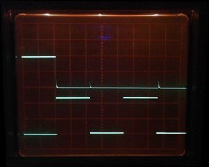
Top trace is the pin13 output, bottom trace is the A control signal at pin 11. Y-axis is 5V/div, I forgot to note what the X-axis is set at, but the frequency at the A input is around 1-2kHz, and the spikes are present at all speeds. Spikes in image are 2VDC, but spikes on other outputs vary up to 6VDC, depending on summing overlap of A, B, & C control signals. Control input signal is 0-7 binary, so frequency A = 2x frequency B = 2x frequency C.
All involved ICs are powered at VDD: +12VDC, VEE & VSS: 0VDC.
Setup:
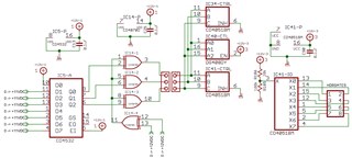
- Incrementing 1-8 decimal count input to IC5, a CD4532BM
- Encoded output goes to IC14, a CD4070BM (used as selectable inverter)
- IC14 output to a pin header to socket header on parallel PCB.
- Socket header to control inputs of three different ICs:
- IC41, the relevant CD4051BM
- IC34, a second CD4051BM (outputs of which drive individual 2N3904 through 10kΩ resistors)
- IC40, a DG408 (used to route ±10VDC signals)
- IC41 has +12VDC connected to Common Out/In pin3, I/O 0-7 each go to individual pins on a pin header that is 0.15" away from the IC.
- Pin header has no further connection.
Attempts to remedy (none had any affect):
- Remove output pin header (outputs now wholly unconnected save for 0.1"-0.2" traces
- Remove IC34 & IC40
- Reduce control signal voltage to 0-9VDC
- replace control input traces with 28ga. wire (traces cut)
The only thing remaining that I can think of is the warning on the data sheet of
"To avoid drawing VDD current when switch current flows into IN/OUT pin, the voltage drop across the bidirectional switch must not exceed 0.6V at TA≤25°C, or 0.4V at TA>25°C (calculated from RON values shown). No VDD current will flow through RL if the switch current flows into OUT/IN pin."
Is this what we're seeing, even though there is no load? If so, what can be done in this situation?
Thanks in advance!
