This thread has been locked.

If you have a related question, please click the "Ask a related question" button in the top right corner. The newly created question will be automatically linked to this question.

SN74CBT3125C: FET Switchi

Part Number: SN74CBT3125C
Other Parts Discussed in Thread: SN74LVC1G139, TS12A44514, TS12A44515, TS12A44513

Hi All,


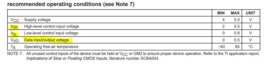
I have a question about SN74CBT3125C.

Is 1B output when VCC and 1A are shorted?
When a voltage of VCC-0.8V or more is input to 1A, is the SW(FET) turned off?


Best Regards,
Ishiwata

  • Hi Ishiwata,

    The device operation is listed in the function table:

    When /OE is low, the associated 1-bit bus switch is ON, and the A port is connected to the B port, When /OE is high, the associated 1-bit bus switch is OFF, and the high-impedance state exists between the A and B ports.

    Is you second question related to when Vcc =0?

    When Vcc is 0 V, the inputs can be any value from -0.5 to 7 V and the outputs will remain at 'high impedance' as the device is fully specified for partial-power-down applications using Ioff.

    Thanks

    Saminah

  • Hi Saminah,

    Thank you for your reply.

    My explanation was not good.

    The customer settings are as follows.

    VCC = 5V
    / OE = Low
    A port = 5V
    B port = not output

    No output from B port in the above case.
    Is B port not output when A port (input) and VCC are the same voltage?


    Best Regards,
    Ishiwata

  • Hi Ishiwata,

    Your supply and Port A input are in the recommended operating conditions - The CBT-C is an NMOS series switch and that it can pass signals only up to a threshold voltage below VCC. So you should see an output on port B at VCC – VT.

    Can you share the schematic of your application

    What is your VIH/VIL voltage 

    Can you short Port A to port B and probe at the output?

    Regards,

    Saminah

  • Hi Saminah,


    Thank you for your reply.

    What is the value of VT? Where is the description of VCC-VT in the data sheet?

    If VCC = 5V and Aport input is 4V, will it be output from B port?
    Is it effective as a measure?

    >Can you share the schematic of your application
    If you want to see the customer's schematic, I will send you a private message.

    >What is your VIH/VIL voltage
    I ask the customer. But what is the background for confirming this?


    Best Regards,
    Ishiwata

  • Hi Ishiwata,

    The Vt (Threshold) voltage is not mentioned in the datasheet - but is related to the structure of the CBT switch which is an NMOS series switch and Vt is the  threshold voltage of NMOS - See more details here on this switch structure in Switches and muxes: What are common switch architectures?

     Vcc = 5V and Input  of  4V is in the recommended operating range so the switch should pass the signal to portB.

    I ask about the VIH and VIL levels because the Voltage levels required on the control pin (OE) for the switch to change the internal signal path needs to be in the recommended operating conditions.

    Please let me know if the details help - you can share the schematic for review at saminah_c@ti.com

    Regards

    Saminah


  • Hi Saminah,


    Thank you for your reply.
    I will send the schematic to your mail address.

    I have a question about the following specifications.


    Is VIO = 5.5V (MAX) acceptable when VCC = 5.5V (MAX)?
    Does VIO have to be lower than VCC?


    Best Regards,
    Ishiwata

  • Hi Ishiwata,

    VIO can go up to 5.5V as highlighted in the recommended operating conditions.

    However, as I explained above the CBT-C switch with NMOS series structure will only be able to pass a signal about 1 V < than the Vcc voltage. Meaning if your input signal on port A is 5.5V, you will see ~4.5V on port B when the switch is ON.

    See more details in the below thread.

    Regards

    Saminah


  • Hi Saminah,


    Thank you for your reply.

    VIH / VIL values are as follows.
    VIH = 2.3V (min)
    VIL = 0.55V (max)

    The input to OE is the output (Y3) of SN74LVC1G139.
    Please confirm the circuit diagram separately sent to your e-mail address.

    There was a proposal of TS12A44514 in the thread sent,
    As an alternative product, does the TS12A44514 work properly with VCC = VIO?


    Best Regards,
    Ishiwata

  • Hi Ishiwata,,

    Thanks for sharing the schematic - I'll review it and get back to you.

    Yes, the TS12A44514  has transmission gate structure and supports rail to rail operation

    See more details here on this switch structure in Switches and muxes: What are common switch architectures?

    Regards

    Saminah

  • Hi Saminah,


    Thank you for your reply. Thank you for your support.

    I want to confirm my understanding.
    TS12A44514 outputs when OE is High.
    TS12A44515 outputs when OE is Low.


    Best Regards,
    Ishiwata

  • Hi Ishiwata,

    The TS12A4451x (TS12A44513/4/5) share the same function table you shared above. When "IN" is Low, NC TO COM or COM TO NC is enabled and when "IN" is High, NO TO COM or COM TO NO path is enabled.

    The main difference is the configuration.

    The TS12A44513 has two normally closed (NC) switches and two normally open (NO) switches, the TS12A44514 has four NO switches, and the TS12A44515 has four NC switches

    Regards

    Saminah