Part Number: TMS570LS0714
Other Parts Discussed in Thread: LAUNCHXL2-TMS57012
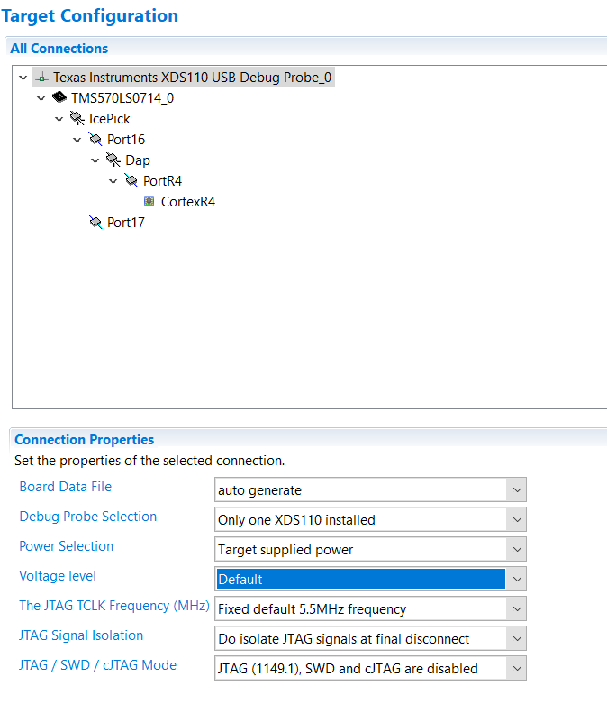
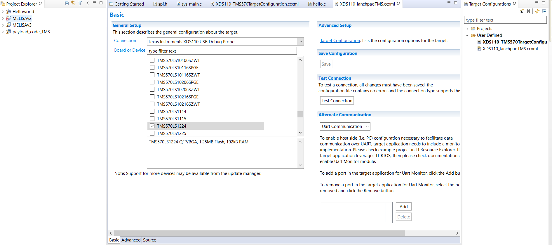
Tool/software: Code Composer Studio
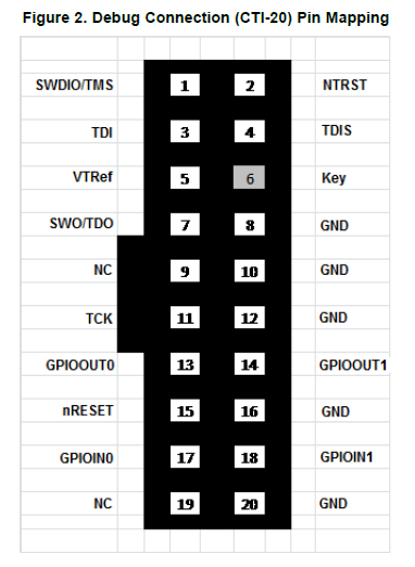
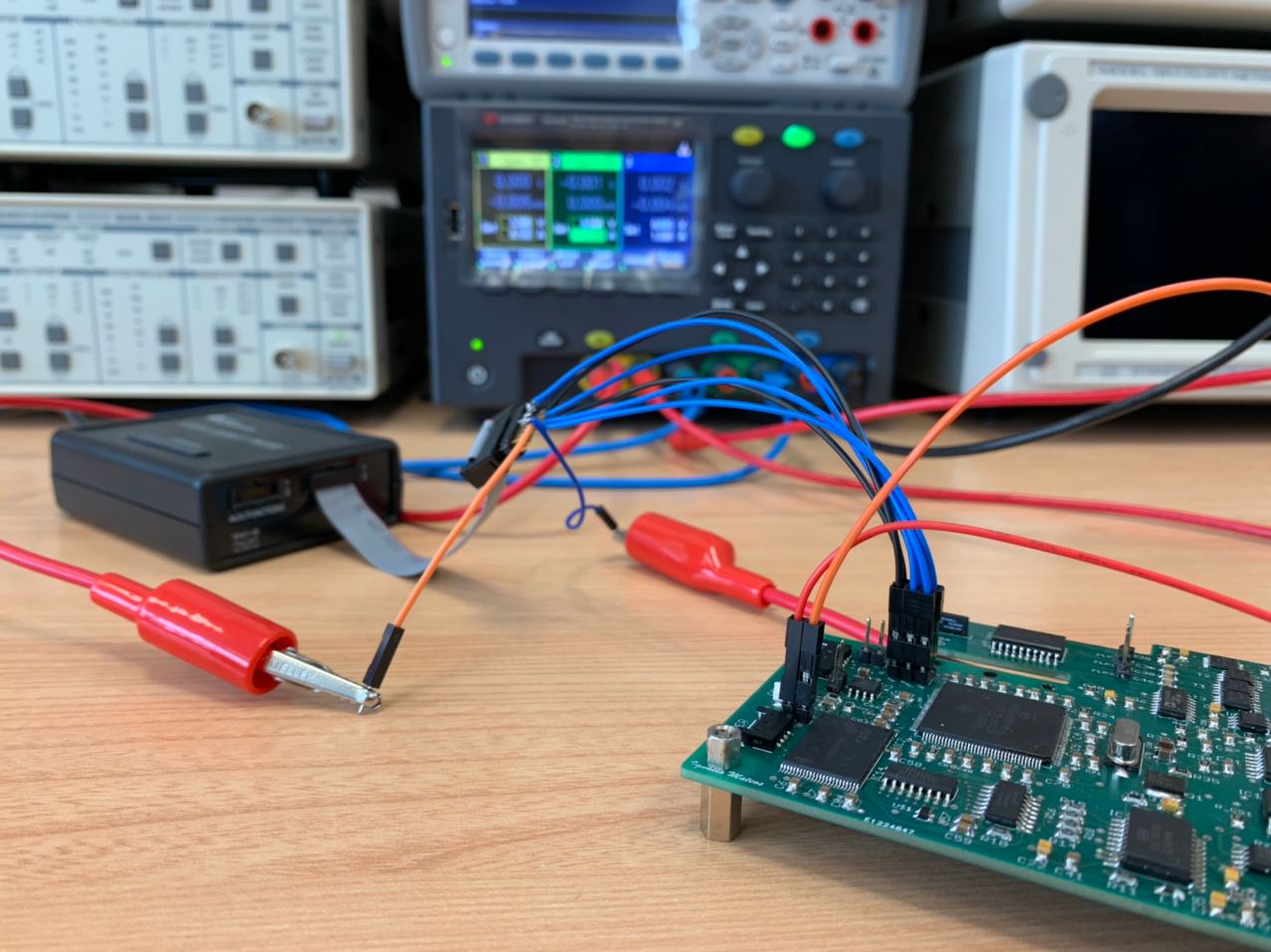
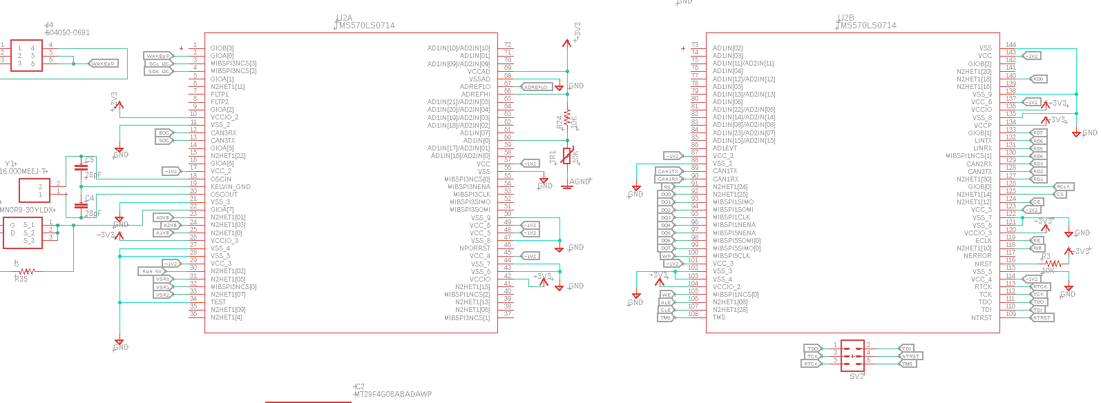
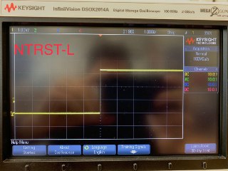
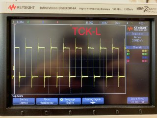
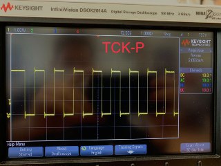
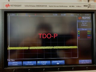
Hello, I am trying to charge a code into a uC TMS570LS0714 using JTAG connection through XDS110 debug probe. I am using the CTI-20 pins connectors as shown in the figure. I show you the configuration I am using as well in the figures. The pinout configuration is the following one:
uC pin XDS CTI-20 pin
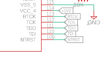
TMS-108 SWDIO/TMS-1
nTRST-109 NTRST-2
TDI-110 TDI-3
TDO-111 SWO/TDO-7
TCK-112 TCK-11
RTCK-113 NONE
3.3 V VTRef-5
GND GND-10
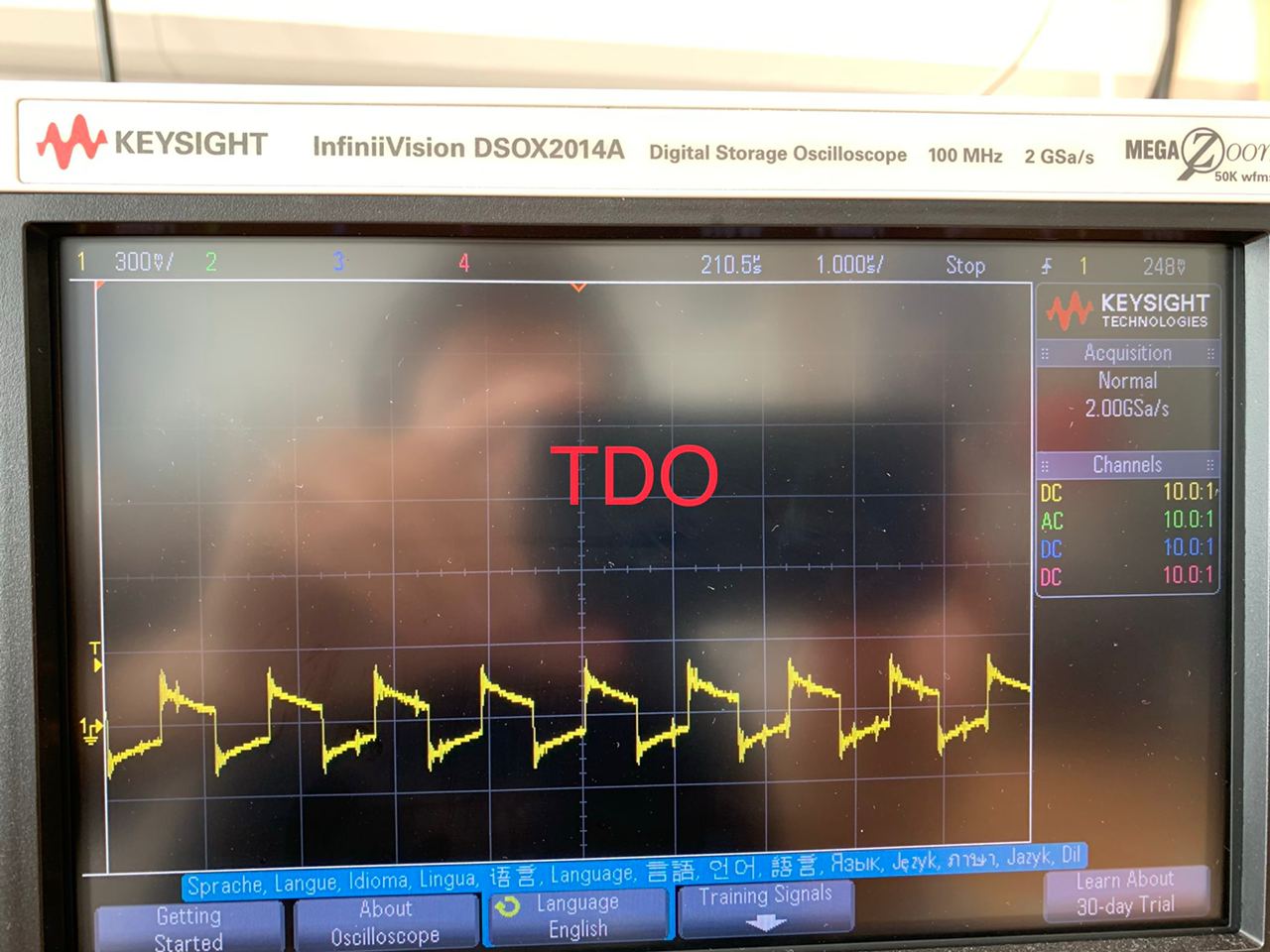
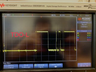
The error I have trying to debug and charge the code on the uC is:
Error connecting to the target:
(Error -2131 @ 0x0)
Unable to access device register. Reset the device, and retry the operation. If error persists, confirm configuration, power-cycle the board, and/or try more reliable JTAG settings (e.g. lower TCLK).
In addition, trying the test connection I get this error:
This error is generated by TI's USCIF driver or utilities.
The value is '-233' (0xffffff17).
The title is 'SC_ERR_PATH_BROKEN'.
The explanation is:
The JTAG IR and DR scan-paths cannot circulate bits, they may be broken.
An attempt to scan the JTAG scan-path has failed.
The target's JTAG scan-path appears to be broken
with a stuck-at-ones or stuck-at-zero fault.
I have checked all the connections and I am powering the XDS debug probe with 3.3V on one side and my target with 6.5 V but thanks to dome DC/DC converters I have 3.3 and 1.2 V for the uC.