This thread has been locked.

If you have a related question, please click the "Ask a related question" button in the top right corner. The newly created question will be automatically linked to this question.

I'm having trouble simulating a buck converter on Tina

Other Parts Discussed in Thread: UCC21530

I'm trying to use a UCC21530 gate driver to simulate a buck converter.

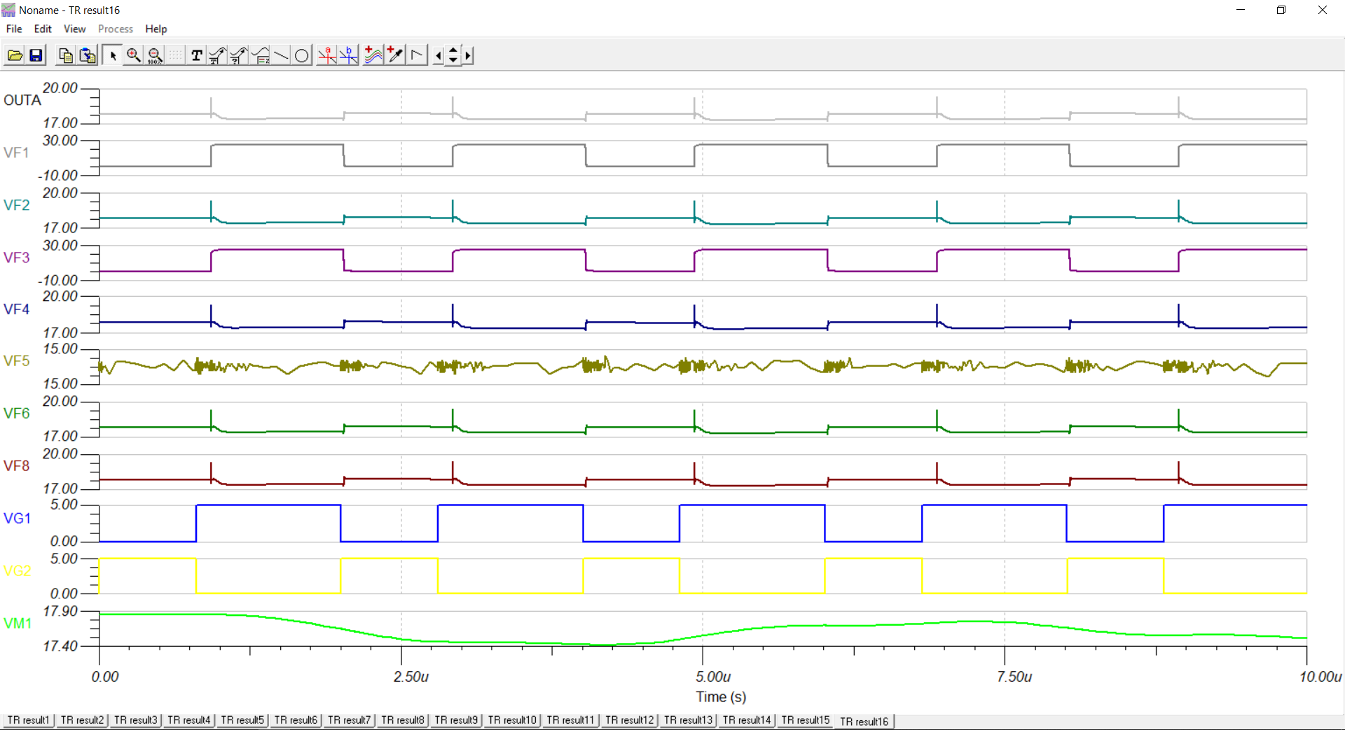
The driver is taking in a square wave input of 5 volts and outputs a square wave of 20V which is used to switch a MOSFET.

The gate driver is operating properly.

The buck converter has a duty ratio of 0.4.

The buck converter works fine as long as the drain voltage of the MOSFET is lower than the gate voltage. If the drain voltage is higher than the gate voltage the output of the transistor is capped at 8 volts which is 40% of the gate voltage. I tried this with different MOSFETs from different companies and they all gave me the same result.

Here is the schematic:

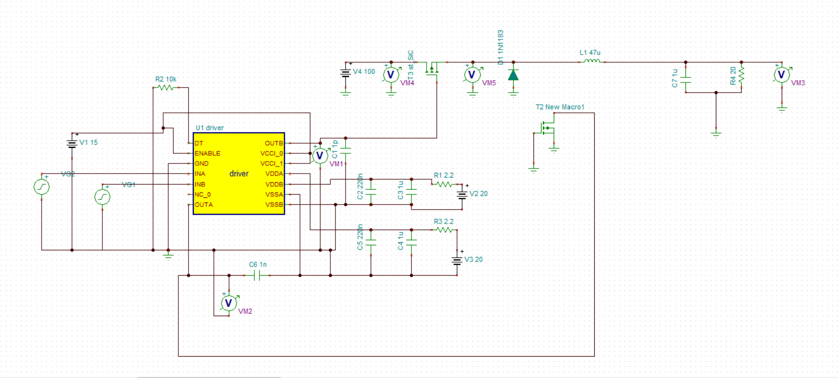
VG1 and Vg2 are the input to the driver.

Vm1 and VM2 are the output from the driver.

VM3 is the output of the converter.

VM4 is the input of the converter

  • Hi Mukund,

    Thank you for your question. I work on the applications team in the high power drivers group.

    Your design is using a ground reference supply for your high side driver.  This is likely what’s causing your issues.  The high side tends to be referenced to the source of your high side MOSFET.  This way the gate drive voltage is increasing your Vgs and turning on the MOSFET.  I can see VM5 (the source), is rising at the same time and by about the same amount of voltage as VM1 (gate), meaning T3 probably isn’t turning on.

    You can reference our typical application section (9.2) in the UCC21530 data sheet for more specific schematic examples.

    https://www.ti.com/lit/ds/symlink/ucc21530.pdf

    If this answered your question, could you please press the green button? If not, feel free to ask more questions.

    Thanks and best regards,

    Zach

  • Hi Zach,

    I tried connecting the converter to the driver as mentioned in the data sheet, but I ran into some other difficulties. I included a bootstrap circuit with the input of the VDD used for the high side FET. The output of the bootstrap circuit is around 17V, which should be fine for the driver. The output to the high side FET is not a square wave but a constant signal of 17V. This means that my high side FET is not switching. If you could take a look at it it would be very helpful.

    Thank you,

    Mukund

    here is the schematic:

    and the waveform:

    here is the .TSC file:

    dan_buck.TSC

  • Hi Mukund,

    It looks like you made some good changes to your circuit since your last post.  You have a wire next to C1 that’s shorting your VDDA and VSSA.  This is why your VF2 and VF8 waveforms (VDDA and VSSA respectively) look the same.  The high side isn’t getting enough voltage across those pins to turn on.  OUTA looks to have a similar waveform to VF4 (the source of the high-side FET), so while the voltage on OUTA is 17 or 18 relative to GND, the Vgs voltage is near zero which is why the FET isn’t turning on.  Deleting that wire next to C1 should resolve your issue.

    The only other cause for concern could be your bootstrap diode (D1), specifically the breakdown voltage.  Setting it to 100V or more should avoid any problems with it breaking down and you losing power for your high side during switching.

    If this answered your question, could you please press the green button? If not, feel free to ask more questions.

    Thanks and best regards,

    Zach

  • Hi Zach,

    Thank you for your reply.

    I removed the wire next to C1 that was shorting VDDA and VSSA but the simulator gave me a convergence error. I tried reducing the capacitance C1 but it didn't help. I'm trying to debug it but I'm not getting anywhere.

    If you could take a look at it, it would be very helpful.

    Thank you,

    Mukund

    0640.dan_buck.TSC

  • Hi Mukund,

    I noticed the source of your T1 transistor is tied to 15V.  It should be tied to ground.

    If you continue to get convergence issues, you should look at altering the TR minimum Time Step parameter to a larger value, around 1ps.  If you still get the convergence error, ignore it and let the simulation continue.  Sometimes there is some high frequency noise in these simulations that can cause the convergence error.

    If this answered your question, could you please press the green button? If not, feel free to ask more questions.

    Thanks and best regards,

    Zach

  • Hi Zach,

    I connected the source of T1 to gnd, but I still get the same error. If i ignore it the simulation just stops.

    How do I change the TR minimum Time Step parameter?

    I went to Analysis => Set Analysis parameters, but I could not find TR minimum Time Step parameter.

    I also couldn't find anything online about it.

    Thanks,

    Mukund

  • Hi Mukund,

    In order to adjust the TR minimum time step parameter. When you go to Analysis parameters, click on the hand button in the lower right and select "View All". Scroll down, it should be near the bottom.

    I took a look at your design file and made the changes I suggested in my previous post, setting the minimum time step to 10ps instead. The simulation will run on my system without a convergence error.

    0640.dan_buck_edit.TSC


    If this answered your question, could you please press the green button? If not, feel free to ask more questions.

    Thank you and best regards,


    Zach