This thread has been locked.

If you have a related question, please click the "Ask a related question" button in the top right corner. The newly created question will be automatically linked to this question.

WEBENCH® Tools: LM3409 FET dimmer

Other Parts Discussed in Thread: LM3409HV, LM3409, TPS92641

Tool/software: WEBENCH® Design Tools

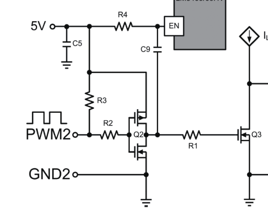
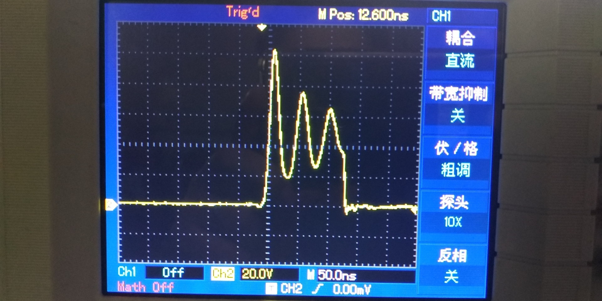
hello,this is a sch from Figure 4. External shunt FET dimming circuit with EN pin coupling of AN-1953 LM3409HV Evaluation Board .I found the EN level is same as R1. EN low  levels means system should shutdown.I have two questions.

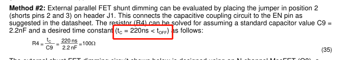
1:C9 is not used for Bootstrap circuit?

2:How to understand FET dimming working with system  shutdown?

  • Hello,

    C9 causes EN to go low for a short time when the Shunt FET opens.  EN should not be low, R4 is 100 ohms and C9 is 2200 pF.  This is a time constant of 220 ns.  EN should not be the same level as R1.

    1)  yes, it causes a short low state when the shunt FET is opened.

    2)  The LM3409 should be enabled when the shunt FET is shorting the LED stack.

    Best Regards,

  • Hello,

    I haven’t heard back from you, I’m assuming you were able to resolve your issue.
    If not, just post a reply below (or create a new thread if the thread has locked due to time-out)

    Best Regards,

  • hello,the blue wave is the R1,the yellow wave is the EN. I used two kinds of PWM.but I also found the EN test point is same as R1.  I know LED "External shunt FET dimming" system not dimmer by EN. but last I also undersand why need introduction C9 for 220ns?why the EN need experience low voltage in "External shunt FET dimming circui" system.

  • I found the system will be more stable in very little PWM Duty cycle with C9(eg. 0.06%Duty cycle  20KHZ). if without C9,the LED will always flashwhy with  little PWM Duty cycle 。why the C9 is so important and specific role in the system? 

  • Hello,

    C9 restarts the PWM cycle.  This is not the preferred method to use when shunt FET dimming.  A second Roff resistor to supply current to the Coff pin is:

    See 8.3.8 and Figure 27 in the datasheet.

    What does your output voltage look like at these very low dimming duty cycles?

    Best Regards,

  • 1:this is LED output wave with mini PWM Duty Cycle

    2:this is LED output wave with more PWM Duty Cycle

    3:I haven trid the sch of Figure 27. External Parallel FET Dimming Circuit. but when I power up,the P mos and N mos all broked.I am afraid so not try again.

  • “C9 restarts the PWM cycle. ”  Can I understand  for this:LM3409 system frequency with N mos dimmer frequency synchronous starting point?


  • Hello,

    I'm not sure what you are asking.  What are you trying to do?  There is a lot of high frequency ringing.  Are you using the EVM or your own board?

    What are the voltage ratings of your Shunt MOSFET?  Your scope is showing around 100V on the output peak during the ringing.

    Best Regards,

  • hello,I used my board,this is my sch,the N mos is 150V voltage ratings.

    I want to make the beads light by very low duty ratio(eg.J2 with 13ns Pulse width).

    1:I test found C8 can make system more stable by low  duty ratio,I want to understand the principle.    

        “C8 restarts the PWM cycle. ”  Can I understand  for this:PMOS working frequency need synchronous with N mos dimmer frequency? but look like tps92641 ,it not used c8 with External Parallel FET Dimming?

    2:what can I do to reduce a lot of high frequency ringing.

    thanks very much.

  • Hello,

    1)  The circuit comprising of C8 in your design was an earlier attempt to recover from when the Shunt FET was closed and Vout went low.  All it is doing is resetting the LM3409 to turn on the switching MOSFET when the EN pulse goes back high.  The correct, or better, fix is the second Roff resistor that keeps the off-timer running when the output is low.  This is mentioned before per Figure 27 and section 8.3.8 in the datasheet.  If your MOSFETs failed it was not implemented correct.  The TPS92641 part was developed later and works different.

    2)  How are the LEDs connected to the LM3409 circuit?  Are there wires?  Ringing is caused by parasitic inductance.  How are you measuring these signals?  The oscilloscope connections cannot have much inductance either.  Have you looked at the drive waveform to see if the measurement is correct?

    Is your design always very low duty cycle?

    Best Regards,

  • hello,

    1)I find a describe "This modification includes 2 extra diodes (i.e. BAT54H) and one resistor (R OFF2 ) and is only relevant when
    shunt FET PWM dimming below 10 kHz or so." from AN-1953 LM3409HV Evaluation Board..But my dimmer PWM frequency is 20kHz. The second Roff resistor circuit can applied to my system ? and the diode can used with look like SS34? 

     if I used shunt FET PWM dimming,which is better with  TPS92641 and LM3409HV from dimmer the dimming effect?

    2) the LEDs connected is wired with J1. The LED- is connet with J1.gnd.   MY testpoint is.NMOS.S as GND, the label "LED+" as test wave. 

       "Ringing is caused by parasitic inductance." ,this is produce by NMOS or 22UH L?


    3)the product is usde for the stage theater,so it need very low light scenario. It won't always be low light, but it may be always be turn off LED by PWM dimmer.

    thank you for your reply.

  • Hello,

    1)  Hysteretic controller can dim to high ratios.  The TPS92641 can also dim to high ratios.  The configuration of your setup is causing issues.  The waveforms need to be corrected before going further.

    2)  The parasitic inductance is cause by "the LEDs connected is wired with J1".  Those wires are causing the ringing you are seeing.  If you look at the voltage across the LEDs, not at the board, it will look different.  Try connecting the LEDs or a different LED load with minimal inductance between the output of the LM3409 circuit and the LEDs.  The Shunt FET should be close to the LED load with minimal trace or wire inductance.

    3)  Some of the EVMs are set up for shunt FET dimming, you may want to get one and try it.

    Best Regards,

  • hello ,I look at AN-1953 again today.

    1:   I want to know if my toff time is set with 242ns,so the tc time need set less than toff time .buy the different tc time whether there are different effects?For example the tc time set 100ns and 200ns .

    2:   I have another question.The yellow is G waveform of NMOS ,the blue is D waveform of NMOS.I found the LED turn on time is slower than turn off time .I want to speed up the LED turn on time,so i try kinds of NMOS to test ,eg. IRF110 .but Not very effective.  Is there any reason why the light turns on slowly?

    Best Regards

  • Hello,

    The two Roff resistors is better suited for shunt FET dimming rather than this circuit.

    The off-time doesn't have anything to do with the C9 time delay.  toff controls how long the switching MOSFET is off during normal operation, with no Shunt FET dimming.  The off-time when shunt FET dimming without the second Roff resistor will put it to maximum off-time since Coff cannot charge.  When the Shunt FET is on, Vo is zero volts in that equation.  Besides you are running from 12V, the off-pulse will be much shorter than a time constant.

    "I have another question.The yellow is G waveform of NMOS ,the blue is D waveform of NMOS.I found the LED turn on time is slower than turn off time .I want to speed up the LED turn on time,so i try kinds of NMOS to test ,eg. IRF110 .but Not very effective.  Is there any reason why the light turns on slowly?"

    What causes the drain to rise?  What causes the drain to fall?  When the shunt MOSFET turns on it can pull a lot of current through the drain path.  When the shunt FET turns off the inductor current is what pulls the drain high, it is not being forced by the Shunt MOSFET.  To speed it up would require less parasitic capacitance across the shunt FET and output.  A MOSFET with less Coss will speed it up provided it is a substantial portion of the parasitic capacitance.  The equation will be I = C * (dv/dt).  I is the inductor current, C is the parasitic capacitance, dv is the output voltage, dt is the slew time.  This will be non-linear since Coss varies with Vds.

    Best Regards,

  • hello,"C9 causes EN to go low for a short time when the Shunt FET opens .". In this time,The  EN voltage goes from low to high.buy how to understand the 3.5 microsecond delay for I_LED don't appear?

    Best Regards,

  • Hello,

    That delay is the turn on after being off for an extended period so the inductor discharges.  The rise time is the time it takes to recharge the inductor.  If it is disabled for a very short time the inductor current does not discharge.  Shunt FET dimming works different though if the LM3409 output is shunted for a long time it will also discharge but at a much slower rate since the inductor is discharging across the freewheel diode instead of the freewheel diode plus the LEDs.  This is why, sometimes, the second Roff is needed.  If the Shunt FET is low long enough the current will decrease resulting in a longer recovery time.

    Best Regards,