This thread has been locked.

If you have a related question, please click the "Ask a related question" button in the top right corner. The newly created question will be automatically linked to this question.

TIDA-00826: PCB related questions

Part Number: TIDA-00826
Other Parts Discussed in Thread: LMX2594, ADC12DJ5200RF, ADC12J4000, ADC12DJ5200RFEVM

Dear team,

Customer wants to know some details about PCB of TIDA-00826:

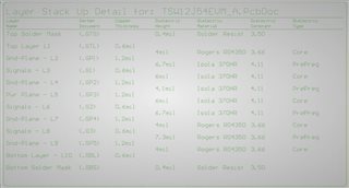
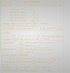
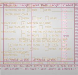
1. Do we have the info of TIDA-00826 stack-up reference materials that could provide to them? Does the PCB board use FR4 or does it use high-frequency RO4003 or other composite boards of the same level?
2. The ADC12DJ5200RFAAV architecture uses LMX2594 as the 5G sampling rate. Do you recommend FR4 or something else for the PCB board? In addition, can the 5G sampling rate differential pair go to the inner layer of the PCB?

Looking forward to your reply.

Thank you.

Best Regards,

Cindy

  • Hello Cindy,

       The PCB PDF layer view and Gerber files are available under design files in the TIDA-00826 product folder. 

       I have attached the stack-up and design layer information for this reference design below:


      From information above, you are correct, the board uses high-frequency layer material, in this case it is the R04350. 

      For the second question, are you referring to a board with just the ADC12DJ5200RFAAV rather than this reference design? 

    Thank you,

    Sima

  • Hi Sima,

    Thanks for your reply.

    Basically customer will copy our reference design and they will change ADC to ADC12DJ5200RFAAV going with LMX2594.

    They're wondering if there're anything else they need to pay attention to when they're building PCB.

    Thank you.

    Best Regards,

    Cindy

  • Hello Cindy,

      Thank you for the further clarification. The ADC12DJ5200RF is faster than the ADC12J4000, there are a more layout precautions to take care of especially making sure the impedances of the traces to the input pins are balanced. It is critical to follow the layout recommendations in the ADC12DJ5200RF datasheet which can be found in section 10.

       Also, I would recommend following the design files of the ADC12DJ5200RFEVM located here. I have attached the layer/design stack up of this EVM below. A lot of care went into the reference design to account for high frequency design, but it is a good idea to be extra cautious around the very high speed ADC. 

    Thank you,
    Sima 

  • Hi Sima,

    Thanks for your explanation in detail.

    One quick question, we see no matter in ADC12DJ5200RF EVM and TIDA-00826, the high speed differential pairs goes at top layers, so customer wants to know if these signal could go to inner layer if they want to avoid signal cross over?

    Thank you.

    Best Regards,

    Cindy

  • Hello Cindy,

      That is a good question. Routing high speed differential pairs in the inner layers does help minimize crosstalk, but this also means the use of more vias near those crucial traces. I will talk to an expert in this, and get back to you with an update by tomorrow.

    Thank you,
    Sima 

  • Hello Cindy,

       This is the answer I received:

    It would be preferred if they refer to the ADC12DJ5200RF EVM for routing on the 5G sampling rate. So, on a first order, the differential pairs would be immune to crosstalk and interference. Routing the differential pairs on an inner layer would add to additional parasitic inductance on the traces which would result in sub optimal differential data rate than 5G. So, they may not be able to get full benefit of the high speed digital data interface.

    Thank you,
    Sima