


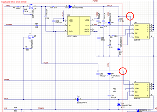
As you can see, the VCC pins of the two GaNs both come from the VDD in the upper left corner, but they have different reference GND, so how are the two GaNs powered?
As you can see, the VCC pins of the two GaNs both come from the VDD in the upper left corner, but they have different reference GND, so how are the two GaNs powered?
