Tool/software:
Hello Team,
When we are trying to run PCM control with CV regulation as per reference design with our own customized design we are observing OUT C & OUT D duty outcome event though we have put required/calculated/recommended circuit in primary CT current sense path as shown below,
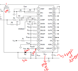
We have done scaled input voltage board bring up with two cases on RFLT & CFLT changes as case 1: 500 Ohm & 680pF and case 2: 1 kOhm & 330 pF (Fcutoff above Fsw-150kHz)
Case 1:
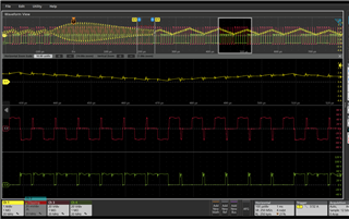
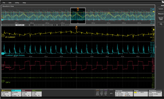
Operational conditions ; Vin 50V , Vout 10V , Iout 0.5A
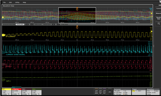
Operational conditions ; Vin 50V , Vout 10V , Iout 4 A
Case 2:
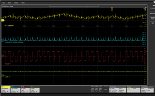
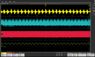
Operational conditions ; Vin 50V , Vout 10V , Iout 0.5A
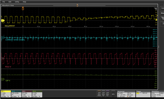
Operational conditions ; Vin 50V , Vout 10V , Iout 4 A
Could you let us know how to improve noise immunity for current sense feedback, so that OUT C & OUT D duty variation above and below 50% avoided as seen in the Pri pole voltage.
Compensator output follows ripple voltage as seen in output voltage (Near 1.1V (+/- 0.1V)), but no drastic swing.
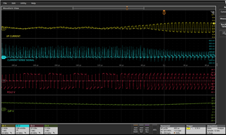
Just as additional input , we did experimentation by removing pri CT feedback signal still observed similar duty variation in OUT C & OUT D as shown below via Pri pole voltage, Vout regulated as set reference.
In below waveform CH3 shows primary pole voltage & CH4 QD drain to source voltage (OUT D) shows duty variation issue of Leg 2 (OUT C & OUT D)