This thread has been locked.

If you have a related question, please click the "Ask a related question" button in the top right corner. The newly created question will be automatically linked to this question.

TIDA-010015: Power supply design not working with low input voltage

Part Number: TIDA-010015
Other Parts Discussed in Thread: UCC256302

Hi ,

We have designed power supply based on TIDA-010015 model (24V output) with new PFC inductor and Transformer for 600W. It is working with full power delivery and efficiency at 230VAC input (direct from socket or Auto transformer) but with low input voltage ( 110VAC) system not working properly and having problem every time while loading.

For 110V AC testing also we used Auto transformer but we are facing issues as below:

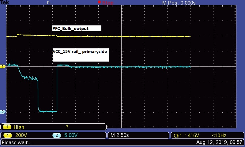
Problem 1. Auto Transformer generates Humming noise even when board operating at 45W load and it keeps on increasing. At one stage board goes to hiccup mode (at 7A).

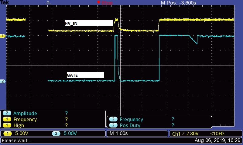
Problem 2. Some time while increasing load, board got problem where active inrush circuit goes bad (MOSFET Q3+ FUSIBLE resistor R12) . (Ref design part : EMC2-47RKI and our design part : PR02FS0204709KR500). We did the testing multiple times and always find active Inrush limiter circuit going bad.


To confirm problem is not there with Auto transformer, we use the same with Meanwell power supply UHP-350-12 for 110V AC and didn't observer any humming noise.

Please share some pointers to start the debugging.

Note: We have a strict requirement for 100-125VAC input for full load.

  • Hi Balasubramani,

    For the audio noise issue, I would suggest minimizing the burst thresholds on both PFC and LLC. This will help with the debug. Depopulate R28 and R66. It would also be good to look at the shape of the input current to determine if there is some distortion that is causing the audio noise. This could happen if there is noise on the pins controlling the switching action (TSET, ZCDA/B, VINAC, etc).

     For the active inrush limit issue, is the MOSFET and resistor getting damaged when AC is first applied or does it only happen when the load is increased? Perhaps the gate of Q3 is not staying properly biased at steady state and the resistor is seeing large ripple current as a result.

    Best Regards,

    Ben Lough

  • Hi Ben,

    We tried to remove R28 (Not LLC Burst setting)  and we observe smooth running under low voltage no noise at all , but loading further with low voltage input not passed yet. This Active inrush mosfet and resistor keeps on dissipating heat and at one stage this MOSFET completely blown. 

    we are using somewhat better specification than the reference design FET. Still we are looking where we are missing). 

    (Note: This Fet getting burnt only at the time of loading and the loading is not more than 25W@24V. )

    Please share your thought. 

    BR,

    Bala.

  • Hi Bala,

    Is the gate to source voltage for the active inrush MOSFET stable and sufficient for keeping the MOSFET biased on? This is to make sure the inrush circuit is correctly biasing the FET at steady state. I would also suggest measuring the drain to source voltage across the MOSFET. This FET will see the output ripple current so perhaps a FET with a better body diode would also help.

    Best Regards,

    Ben Lough

  • Hi Ben,

    As per your suggestion the FET should be biased always for inrush protection . But we have measured and found this waveform. This not stable for every half cycle the opamp keep on shifting high and low. 

    CH1- VDS CH2-Gate

    This is for 230VAC.

    At 115VAC_ Fet Gate vs HV voltage

    CH1- HV voltage CH2- Gate

    At 230VAC_ Fet Gate vs HV voltage

    CH1- HV voltage CH2- Gate

    Let me know how to proceed further.

  • Hi Bala,

    I would suggest comparing the voltages on the input pins to the op-amp. The voltage on pin 4 should be fixed at 5.1V. The voltage on pin 3 should be a divided down version of the average AC voltage. From what I can tell from the waveforms, it looks like perhaps more margin is needed on divided down AC voltage. I would suggest increasing R11 to 60.4kΩ and also increase C12 to 220nF so that the pin 3 waveform does not have so much AC ripple. 

    Best Regards,

    Ben Lough

  • Hi Ben,

    Thanks For the input. It really helps well. Now we could analyze the issue and root cause for the issue. We changes the values to 60k and 220nf and still we could see some inconsistent in gate below 105VAC.  so i have added again another 220nf in C12 (220nF + 220nF)  to make it work and i could observe change in sequence in the gate side. How to over come this issue ?

    May i know why this changes required in spite of same circuit used in almost most of the TI power supply design. Why im asking this question is ,  in future whether we will have same issue and again do we need to tune the value?

    Please help here to understand better. 

  • Hi Bala,

    The designer of TIDA-010015 likely was using the peak of the AC line for the AC divider calculations. This would have yielded 5.6V at 85Vac input and R76 in the TI schematic equal to 49.9kΩ. In practice, I believe you are more likely to see the average of the rectified AC line at the comparator pin which is equal to 2*Vac_peak/pi. Using 60kΩ for the bottom resistor and 105Vac input, this would present 5.24V at the comparator input pin which is much closer to what you are seeing in your design. I will check with the reference design engineer to clarify.

    Regarding the new waveform you shared, is this during startup or steady state condition? If the gate low period is when VCC is charging up then I would say it is ok because the LLC will not begin switching until BLK is above the BLKStart threshold and VCC has finished charging up to 26V. There would be no load on the PFC converter during this time.

    Best Regards,

    Ben Lough

  • HI Ben,

    I hope changing the threshold according to the low input peak will not cause any issue and i got the point of TI design settings. 

    And this sequence observed only at the startup time. I hope this also not problem hereafter. 

    Thanks for the clarification and support, expecting Designer's reply one last time as you told earlier. 

  • Hi Bala,

    I sent a message to the designer. I'm hoping to have a conclusion to the AC divider question within the next day or so and will share the designer's input with you as soon as it is available.

    Best Regards,

    Ben Lough

  • Hi Bala,

    I had a chance to talk to the designer and he mentioned he was already in contact with your team discussing this. I believe this issue is now solved. If there is anything else you need from my end, just let me know.

    Best Regards,

    Ben Lough

  • Hi Ben,

    We further modified the values in the comparator input now it is working upto the design requirement , But we are facing some peculiar issue like while disconnecting the load (electronic load turned off ), board getting restarted. This is happening almost 5 out of 2 boards. This power supply board output goes to less than 15v and again getting steady at 24V. 

  • Hi Bala,

    What I suspect is that the act of disconnecting the load is similar to a transient response going from heavy load to light load. The LLC will stop switching and wait for the output to fall back to the regulation set point before resuming switching. While the converter is not switching, the VCC voltage does not get replenished from the bias winding. What I suspect is that the VCC is dropping to the 10.5V restart threshold on VCC which would make the controller turn its HV startup back on, recharge VCC and then go through soft start. The output is likely dropping to 15V because while the controller is charging up the VCC capacitance, the controller is not switching so the output voltage continues to droop. I would suggest probing the VCC voltage and if the voltage is indeed dropping to 10.5V, try increasing the capacitance some.

    Best Regards,

    Ben Lough

  • Hi Ben,

    I checked this rail and found whenver this load transient (Full to No load ) there is a dip in the 15V rail and also we could observe this PFC voltage goes above 420V at some instance. 

    can you guide me why this LLC stop switching ? what is the reason in dip in this VCC_15V rail. We are out of idea why this 15V rail goes below 10.5v? 

    Please help here to clear the issue. 


  • Hi Bala,

    The LLC stops switching because going from heavy load to no load looks like a load transient. The controller is waiting for the output voltage to droop back to the regulation set point before resuming switching. There are a couple ways we could address this. We could increase the VCC capacitance more to have more charge for the controller to live off of while the controller waits for the output to droop down. We could also place a small resistor dummy load on the output so that when going from heavy load to no load, the output voltage will droop down to the regulation set point faster and the controller will resume switching before running out of charge on VCC.

    Best Regards,

    Ben Lough

  • HI Ben,

    We moved to UCC256302 LLC IC since we have a requirement with DC input to our power supply since this UCC25630-1 have Xcap discharge function we decided to use UCC25630-2 IC with external Xcap discharge mechanism, with that restarting problem not there in this new IC. But while we adjusted the VINAC settings accordingly to make it work within the range of 100V-120VDC.we are facing some new issue like 

    It is working fine with DC but for AC we have regulation problem at output voltage. 

    With DC input we could achieve all power what we designed and the output regulation with in 1% @24v.

    With AC input we could able to achieve only 85% load , if we increasing more than 85% load the output voltage decreased to 20V.

    Again we reverted this VINAC and then we checked it deliver almost only 1.5% output regulation for AC input. 

    What could go wrong if we change the VINAC settings and it affects only AC based input voltage. 

    Could you help here? 


  • Hi Bala,

    It sounds like the VCR pin is running out of headroom. Could you take a look at the VCR pin peak to peak voltage? If it is >=6V, could you increase the capacitance between VCR and ground (C44)?

    Best Regards,

    Ben Lough

  • HI Ben,

    I will check the VCR voltage but my doubt is, at DC input we could get full load with 1% output voltage regulation . How it will be linked with AC input , still we are out of idea. Is VINAC anyway linked with the output section? 

    If I dont adjust any changes in the VINAC we will not face any issue at all (Only at DC source, will start work after 125VDC or so)

    Can you help here to understand this link please.  

  • Hi Bala,

    After changing the VINAC divider, do you see the PFC output voltage droop when the load is greater than 85%? Perhaps the PFC is going into current limit which is causing the PFC bus to droop and making it difficult for the LLC to maintain regulation.

    Best Regards,

    Ben Lough

  • Hi Ben ,

    Yes .. This PFC voltage dropped to 315VDC or so when this problem occurs. (Output voltage regulation problem occurs)

    Note: This only happens when i adjusted the VINAC divider, otherwise if im using same as reference no drop at PFC/VOUT at all.

  • Hi Bala,

    I would suggest checking the CS pin voltage and look if the voltage is exceeding the OCP threshold. This would explain the dip in output voltage. Adjusting the VINAC divider changes the Kt used to calculate the on time. It sounds like a larger on time was being used which caused the PFC controller to go into overcurrent limit.

    Best Regards,

    Ben Lough

  • Hi Ben,

    We have requirement that this power supply should work with both AC and DC input in the range of 100-120V AC/DC. So by adjusting this VINAC only we could able to run the board at DC source.

    What should be the maximum ON time for this PFC switching frequency? 

    Is there any other setting to do this so that it will work both AC and DC source.  So that we can maintain minimum ON time to avoid this over loading. 

  • Hi Bala,

    I would suggest resizing the current sense resistance to avoid going into OCP at minimum input voltage and full load. This would be the most straightforward change. I would suggest first to check the CS pin voltage is exceeding the OCP threshold to confirm this is indeed why the output voltage is drooping at heavy load at low input voltage.

    Best Regards,

    Ben Lough

  • HI Ben,

    This is the observation. We have measured the voltage across CS pin it is 41mV for 110VAC @ full load and 23.6mV for 220VAC @ full load. seems we are good with the CS pin threshold as it is within the range. And we measured the TON time at full load as it comes nearly 15uS at the time secondary side voltage is nearly 22.2VDC.

    Can you guide us where we want to check to overcome this voltage drop issue . 

  • Hi Bala,

    Thanks for the additional information. Could you measure the COMP pin voltage and VINAC pin voltage at heavy load? Is COMP oscillating or stable? What is its voltage? Is the COMP voltage getting clamped at 4.95V? If COMP is oscillating, it could be a compensation issue. If it is a stable voltage, then the VINAC voltage would allow us to calculate the maximum ON time the device is using. 

    Best Regards,

    Ben Lough

  • Hi Bala,

    If the PFC controller is hitting the maximum on time something we could try is slightly reducing the TSET resistor to allow for a longer on time. 

    Best Regards,

    Ben Lough

  • Hi Ben,

    Yes. Found issue with TSET resistor values. We have corrected the values and the problem solved now. Thanks for your extended support.