This thread has been locked.
If you have a related question, please click the "Ask a related question" button in the top right corner. The newly created question will be automatically linked to this question.
Tool/software: WEBENCH® Design Tools
Hello,
Namskar,
I have designed DC -DC 24V to 5V supply. and we are follow TI WEBENCH design. but when load is connected then O/P is 0V.
WithOut Load condition :
1) Vin = 24V and O/P : 5V : R1 = 44.2K & R7 = 2.1K (FB pin Voltage = 1.3V)
2) Vin = 24V and O/P : 5V : R1 = 95K & R1 = 1.43K (FB pin Voltage = 1.3V)
With Load condition :
1) Vin = 24V and O/P : R1 = 44.2K & R7 = 2.1K When Load 3A to 500mA (FB pin Voltage = 0V)
2) Vin = 24V and O/P : R1 = 95K & R1 = 1.43K When Load 3A to 500mA (FB pin Voltage = 0V)
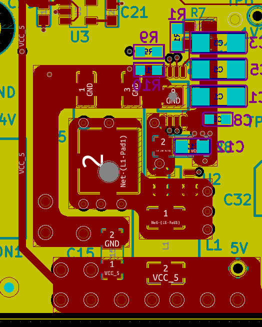
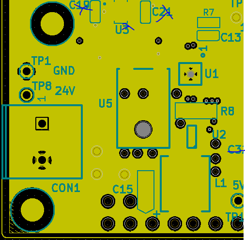
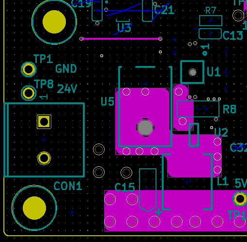
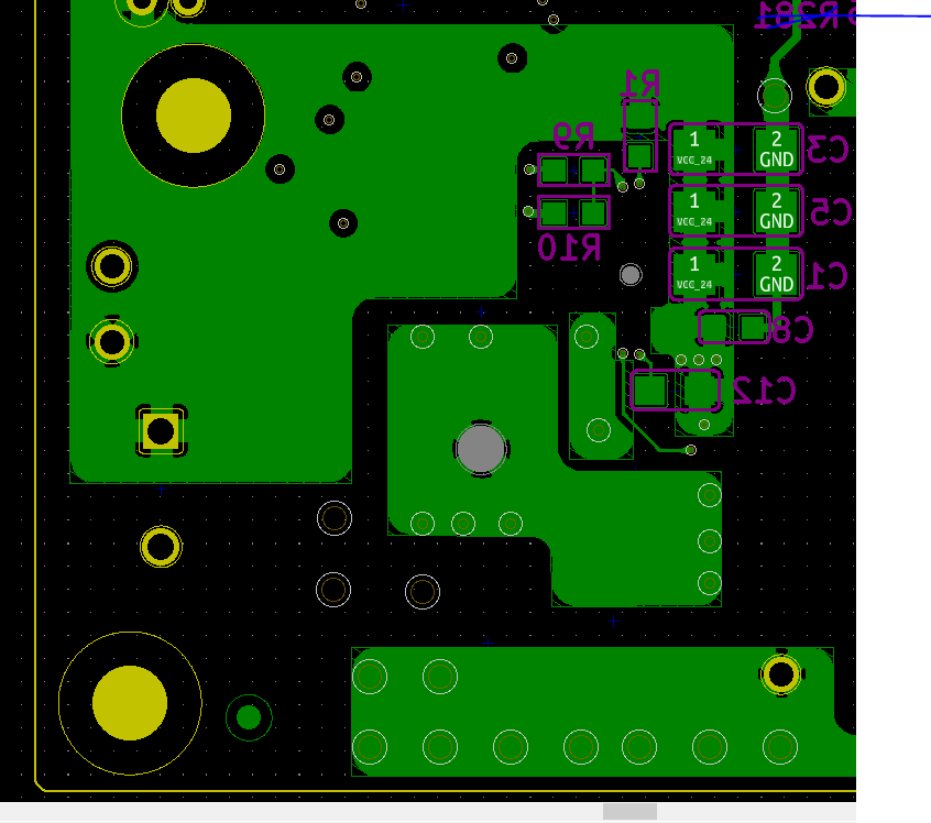
Schematic :
Layout :
Kindly possible to get quick help in regard of this issue.
Thanks in advance.
Hi Chirag ,
We have requested concerned expertise to look into your query.
The snapshots you have shared are not uploaded properly. Can you upload it again.
Regards,
Atul
Hi,
It looks the PGATE path is too narrow, gate driver current is going through it, could you please replace it with a short wire and test it again?
Hi Iven,
Thanks for support.
OK, I will check and let you know about this.
Best Regards,
Chirag Rana
Hi Iven,
Thanks for support,
I have check as gave your suggestion but still issue is not resolved.
If you have any other suggestions resolving this issue, kindly suggest to us.
Best Regards,
Chirag Rana
Hi,
Could you please check if the input source is current limited? What's the heaviest load it can deliver?
Hi,
We has used for testing input source supply is 2A maximum.
Regards,
Chirag Rana
Hi,
What's the heaviest load the circuit can deliver? Could you please probe switching voltage and inductor current waveforms under normal and abnormal conditions? Thanks.