This thread has been locked.

If you have a related question, please click the "Ask a related question" button in the top right corner. The newly created question will be automatically linked to this question.

CC2652RSIP: Antenna Matching pi circuit

Part Number: CC2652RSIP

Dear Team,

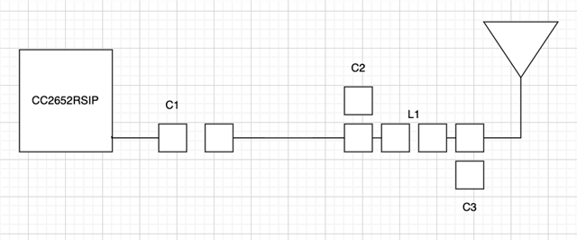
I have LP-CC2652RSIP demo board.

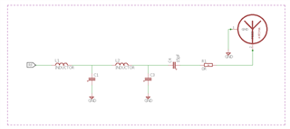
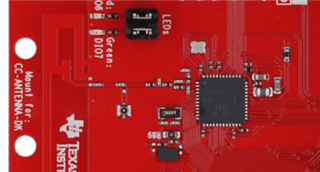
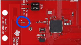
It have not any matching circuit for antenna, there is only one capacitance I think it is for DC blocking.

In SYSCFG file front end mode: differential, Bias confugiration: Internal Bias

In datasheet

"Tuning of the antenna impedance π matching network is recommended after manufacturing of the PCB to account for PCB parasitics."

May I design any pi matching circuit, if I do, how I change settings?

may you give me some details?

Best wishes.

  • Hi,

    While our LP-CC2652RSIP does not have matching circuitry, we do recommend that customer designs using the CC2652RSIP still include that matching in case your impedance is not exactly 50 ohms (which can happen frequently). Look at the LAUNCHXL-CC26X2R1 design for an example of this. You do not need to change any settings in software depending on your matching circuit.

    Best,

    Nate

  • Hi,

    The referance design which you send, is have balun circuitry.

    CC2652RSIP have it on chip.

    So I draw this.

    Best Wishes.

  • Hi,

    You're correct that there is a balun and an LC filter in the reference for the CC2652 I listed above. You don't need all of this. I would recommend you place the 15 pF capacitor before the matching network (replace L1 with C4, remove C4). Then remove the 0 ohm resistor (R1) and place the matching network (the Pi filter composing C1, L2 and C2) as close to the antenna as possible in the layout. This will allow you to tune your antenna appropriately without unnecessary extra components.

    Best,

    Nate

  • Hi,

    Thank you for your helping

    İs this OK?

    Best wishes.

  • No. Please mimic the layout found in the LAUNCHXL-CC26X2 reference design, which places the series component straight on the RF path, and lines the parallel components on opposite sides of the RF path. I would also  Also see section 4.3 of the Design Consideration Guide, which still applies here.

    I would also place C1 and C2 perpendicular to one another, and further apart. See drawing below

  • Hi,

    You said that

    "place the matching network (the Pi filter composing C1, L2 and C2) as close to the antenna as possible in the layout."

    But there is two demo board matching network is close to chip not anttenna.

    I am a little confused.

    LAUNCHXL-CC26X2 reference design

    --------------------------

    Best wishes

  • Hi,

    In this reference design, the matching network is right next to the antenna. I can see how this may be confusing because it doesn't appear to look like a Pi network, but in reality, it is a Pi network with one parallel component DNP-ed and one parallel component missing. When this board was designed, it appears that the antenna match did not require any parallel components, so the series component is the only one necessary to match it.

    I think the components you're referring to are the LC filter and the balun, both of which are integrated into the package for the CC2652RSIP device. So, you don't have to worry about them.

    Best,

    Nate